TDA8922C
NXP Semiconductors
2 × 75 W class-D power amplifier
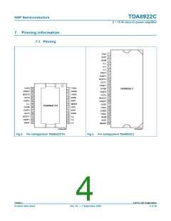
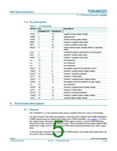
7.2 Pin description
Table 3.
Symbol Pin
TDA8922CTH TDA8922CJ
Pin description
Description
VSSA
SGND
VDDA
IN2M
1
2
3
4
5
6
18
19
20
21
22
23
negative analog supply voltage
signal ground
positive analog supply voltage
channel 2 negative audio input
channel 2 positive audio input
IN2P
MODE
mode selection input: Standby, Mute or Operating
mode
OSC
IN1P
IN1M
n.c.
7
1
oscillator frequency adjustment or tracking input
channel 1 positive audio input
channel 1 negative audio input
not connected
8
2
9
3
10
11
12
13
4
n.c.
5
not connected
n.c.
6
not connected
PROT
7
decoupling capacitor for protection (OCP)
channel 1 positive power supply voltage
channel 1 bootstrap capacitor
channel 1 PWM output
VDDP1 14
BOOT1 15
8
9
OUT1
16
10
11
12
-
VSSP1 17
channel 1 negative power supply voltage
decoupling of internal stabilizer for logic supply
not connected
STABI
n.c.
18
19
VSSP2 20
OUT2 21
13
14
15
16
17
channel 2 negative power supply voltage
channel 2 PWM output
BOOT2 22
VDDP2 23
channel 2 bootstrap capacitor
channel 2 positive power supply voltage
negative digital supply voltage
VSSD
24
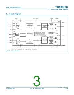
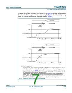
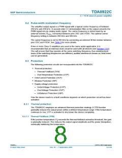
8. Functional description
8.1 General
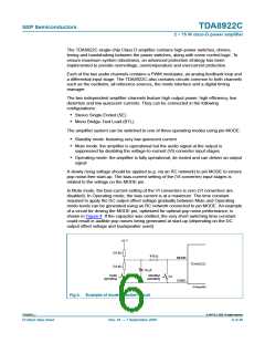
The TDA8922C is a two-channel audio power amplifier that uses Class D technology.
For each channel, the audio input signal is converted into a digital Pulse Width Modulation
(PWM) signal using an analog input stage and a PWM modulator; see Figure 1. To drive
the output power transistors, the digital PWM signal is fed to a control and handshake
block and to high- and low-side driver circuits. This level-shifts the low-power digital PWM
signal from a logic level to a high-power PWM signal switching between the main supply
lines.
A second order low-pass filter converts the PWM signal to an analog audio signal that can
be used to drive a loudspeaker.
TDA8922C_1
© NXP B.V. 2009. All rights reserved.
Product data sheet
Rev. 01 — 7 September 2009
5 of 40

 NXP [ NXP ]