TDA8922C
NXP Semiconductors
2 × 75 W class-D power amplifier
4. Quick reference data
Table 1.
Quick reference data
Symbol Parameter
General
Conditions
Min
Typ
Max
Unit
[1]
[2]
VDD
VSS
supply voltage
Operating mode
Operating mode
12.5 30
32.5
−32.5
70
V
V
V
negative supply voltage
−12.5 −30
Vth(ovp) overvoltage protection threshold
voltage
VDD − VSS
65
-
Iq(tot)
total quiescent current
Operating mode; no load; no filter;
no RC-snubber network connected
-
40
70
-
mA
W
Stereo single-ended configuration
Po output power
[3]
[3]
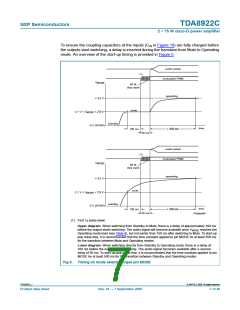
Tj = 85 °C; LLC = 22 µH; CLC = 680 nF (see
Figure 10); RL = 6 Ω; THD + N = 10 %;
-
-
75
VDD = 30 V; VSS = −30 V
Mono bridge-tied load configuration
Po output power
Tj = 85 °C; LLC = 22 µH; CLC = 680 nF (see
Figure 10); RL = 8 Ω; THD + N = 10 %;
155
-
W
VDD = 25 V; VSS = −25 V
[1] VDD is the supply voltage on pins VDDP1, VDDP2 and VDDA.
[2] VSS is the supply voltage on pins VSSP1, VSSP2, VSSA and VSSD.
[3] Output power is measured indirectly; based on RDSon measurement; see Section 13.3.
5. Ordering information
Table 2.
Ordering information
Type number
Package
Name
Description
Version
TDA8922CJ
DBS23P
HSOP24
plastic DIL-bent-SIL power package; 23 leads (straight lead length 3.2 mm) SOT411-1
TDA8922CTH
plastic, heatsink small outline package; 24 leads; low stand-off height
SOT566-3
TDA8922C_1
© NXP B.V. 2009. All rights reserved.
Product data sheet
Rev. 01 — 7 September 2009
2 of 40

 NXP [ NXP ]