TDA8922C
NXP Semiconductors
2 × 75 W class-D power amplifier
20. Contents
1
2
3
4
5
6
General description . . . . . . . . . . . . . . . . . . . . . . 1
16
16.1
Soldering of through-hole mount packages. 37
Introduction to soldering through-hole
mount packages. . . . . . . . . . . . . . . . . . . . . . . 37
Soldering by dipping or by solder wave . . . . . 37
Manual soldering . . . . . . . . . . . . . . . . . . . . . . 37
Package related soldering information. . . . . . 38
Features . . . . . . . . . . . . . . . . . . . . . . . . . . . . . . . 1
Applications . . . . . . . . . . . . . . . . . . . . . . . . . . . . 1
Quick reference data . . . . . . . . . . . . . . . . . . . . . 2
Ordering information. . . . . . . . . . . . . . . . . . . . . 2
Block diagram . . . . . . . . . . . . . . . . . . . . . . . . . . 3
16.2
16.3
16.4
17
Revision history . . . . . . . . . . . . . . . . . . . . . . . 38
7
7.1
7.2
Pinning information. . . . . . . . . . . . . . . . . . . . . . 4
Pinning . . . . . . . . . . . . . . . . . . . . . . . . . . . . . . . 4
Pin description . . . . . . . . . . . . . . . . . . . . . . . . . 5
18
Legal information . . . . . . . . . . . . . . . . . . . . . . 39
Data sheet status . . . . . . . . . . . . . . . . . . . . . . 39
Definitions . . . . . . . . . . . . . . . . . . . . . . . . . . . 39
Disclaimers. . . . . . . . . . . . . . . . . . . . . . . . . . . 39
Trademarks . . . . . . . . . . . . . . . . . . . . . . . . . . 39
18.1
18.2
18.3
18.4
8
8.1
8.2
8.3
8.3.1
8.3.1.1
8.3.1.2
8.3.2
8.3.3
8.3.4
8.4
Functional description . . . . . . . . . . . . . . . . . . . 5
General. . . . . . . . . . . . . . . . . . . . . . . . . . . . . . . 5
Pulse-width modulation frequency . . . . . . . . . . 8
Protection . . . . . . . . . . . . . . . . . . . . . . . . . . . . . 8
Thermal protection . . . . . . . . . . . . . . . . . . . . . . 8
Thermal FoldBack (TFB) . . . . . . . . . . . . . . . . . 8
OverTemperature Protection (OTP) . . . . . . . . . 9
OverCurrent Protection (OCP) . . . . . . . . . . . . . 9
Window Protection (WP). . . . . . . . . . . . . . . . . 10
Supply voltage protection . . . . . . . . . . . . . . . . 11
Differential audio inputs . . . . . . . . . . . . . . . . . 11
19
20
Contact information . . . . . . . . . . . . . . . . . . . . 39
Contents. . . . . . . . . . . . . . . . . . . . . . . . . . . . . . 40
9
Limiting values. . . . . . . . . . . . . . . . . . . . . . . . . 12
Thermal characteristics. . . . . . . . . . . . . . . . . . 13
Static characteristics. . . . . . . . . . . . . . . . . . . . 13
10
11
12
Dynamic characteristics . . . . . . . . . . . . . . . . . 14
Switching characteristics . . . . . . . . . . . . . . . . 14
Stereo SE configuration characteristics . . . . . 15
Mono BTL application characteristics. . . . . . . 16
12.1
12.2
12.3
13
Application information. . . . . . . . . . . . . . . . . . 17
Mono BTL application. . . . . . . . . . . . . . . . . . . 17
Pin MODE. . . . . . . . . . . . . . . . . . . . . . . . . . . . 17
Estimating the output power . . . . . . . . . . . . . . 17
Single-Ended (SE) . . . . . . . . . . . . . . . . . . . . . 17
Bridge-Tied Load (BTL) . . . . . . . . . . . . . . . . . 18
External clock . . . . . . . . . . . . . . . . . . . . . . . . . 18
Heatsink requirements . . . . . . . . . . . . . . . . . . 18
Pumping effects . . . . . . . . . . . . . . . . . . . . . . . 20
Application schematic. . . . . . . . . . . . . . . . . . . 21
Curves measured in reference design
13.1
13.2
13.3
13.3.1
13.3.2
13.4
13.5
13.6
13.7
13.8
(demonstration board) . . . . . . . . . . . . . . . . . . 23
14
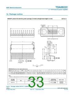
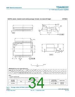
Package outline . . . . . . . . . . . . . . . . . . . . . . . . 33
15
Soldering of SMD packages . . . . . . . . . . . . . . 35
Introduction to soldering . . . . . . . . . . . . . . . . . 35
Wave and reflow soldering . . . . . . . . . . . . . . . 35
Wave soldering . . . . . . . . . . . . . . . . . . . . . . . . 35
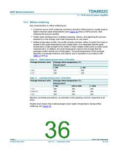
Reflow soldering . . . . . . . . . . . . . . . . . . . . . . . 36
15.1
15.2
15.3
15.4
Please be aware that important notices concerning this document and the product(s)
described herein, have been included in section ‘Legal information’.
© NXP B.V. 2009.
All rights reserved.
For more information, please visit: http://www.nxp.com
For sales office addresses, please send an email to: salesaddresses@nxp.com
Date of release: 7 September 2009
Document identifier: TDA8922C_1

 NXP [ NXP ]