P5CD016/021/041/051 and P5Cx081
NXP Semiconductors
Secure dual interface and contact PKI smart card controller
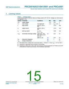
7. Limiting values
Table 5.
Limiting values
In accordance with the Absolute Maximum Rating System (IEC 60134). Voltages are referenced to
VSS (ground = 0 V).
Symbol Parameter
Conditions
Min
−0.5
−0.5
-
Max
Unit
V
VDD
VI
supply voltage
input voltage
input current
+6.0
any signal pad
VDD + 0.5
±15.0
V
II
pad IO1, IO2 or
IO3
mA
IO
output current
pad IO1, IO2 or
IO3
-
-
-
±15.0
±100
±4.0
mA
mA
kV
Ilu
latch-up current
VI < 0 V
or VI > VDD
[1]
VESD
electrostatic discharge voltage pads VDD, VSS,
CLK, RST_N, IO1,
IO2, IO3
[1]
[2]
[3]
pads LA, LB
total power dissipation
-
-
-
±2.0
kV
W
Ptot
Tstg
1
-
storage temperature
°C
[1] MIL Standard 883-D method 3015; human body model; C = 100 pF, R = 1.5 kΩ; Tamb = −25 °C to +85 °C.
[2] Depending on appropriate thermal resistance of the package.
[3] Depending on delivery type, refer to NXP Semiconductors General Specification for 8” Wafers and to NXP
Semiconductors Contact & Dual Interface Chip Card Module Specification.
P5CD016_021_041_51_Cx081_FAM_SDS
All information provided in this document is subject to legal disclaimers.
© NXP B.V. 2011. All rights reserved.
Product short data sheet
PUBLIC
Rev. 3.2 — 14 March 2011
150332
15 of 20

 NXP [ NXP ]