LPC546xx
NXP Semiconductors
32-bit ARM Cortex-M4 microcontroller
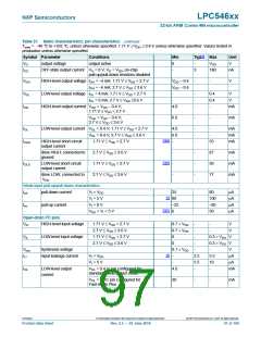
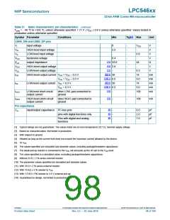
Table 21. Static characteristics: pin characteristics …continued
Tamb = 40 C to +105 C, unless otherwise specified. 1.71 V VDD 3.6 V unless otherwise specified. Values tested in
production unless otherwise specified.
Symbol Parameter
Conditions
Min
Typ[1] Max
Unit
USB0_DM and USB0_DP pins
VI
input voltage
0
-
-
-
-
-
-
-
-
VDD
-
V
VIH
VIL
HIGH-level input voltage
LOW-level input voltage
hysteresis voltage
2.0
-
V
0.8
-
V
Vhys
Zout
VOH
VOL
IOH
0.4
33.0
2.8
-
V
[11]
[12]
output impedance
44
-
Ω
HIGH-level output voltage
LOW-level output voltage
V
[13]
0.3
74
9.0
74
9.0
100
V
[9][10]
[10][11]
[9][10]
[10][11]
[10]
HIGH-level output current VOH = VDD 0.3 V
VOH = VDD 0.3 V
38
6.0
38
6.0
-
mA
mA
mA
mA
mA
IOL
LOW-level output current VOL = 0.3 V
VOL = 0.3 V
-
IOLS
IOHS
LOW-level short-circuit
output current
drive LOW; pad connected to
ground
-
-
[10]
HIGH-level short-circuit
output current
drive HIGH; pad connected to
ground
-
100
mA
Pin capacitance
Cio
input/output capacitance I2C-bus pins
[8]
[6]
[6]
-
-
-
-
-
-
6.0
2.0
7.0
pF
pF
pF
pins with digital functions only
Pins with digital and analog
functions
[1] Typical ratings are not guaranteed. The values listed are at room temperature (25 C), nominal supply voltage.
[2] Based on characterization. Not tested in production.
[3] With respect to ground.
[4] Allowed as long as the current limit does not exceed the maximum current allowed by the device.
[5] To VSS
.
[6] The values specified are simulated and absolute values, including package/bondwire capacitance.
[7] The weak pull-up resistor is connected to the VDD rail and pulls up the I/O pin to the VDD level.
[8] The value specified is a simulated value, excluding package/bondwire capacitance.
[9] Without 33 Ω 2 % series external resistor.
[10] The parameter values specified are simulated and absolute values.
[11] With 33 Ω 2 % series external resistor.
[12] With 15 KΩ 5 % resistor to VSS
.
[13] With 1.5 KΩ 5% resistor to 3.6 V external pull-up.
[14] Guaranteed by design, not tested in production.
LPC546xx
All information provided in this document is subject to legal disclaimers.
© NXP Semiconductors N.V. 2018. All rights reserved.
Product data sheet
Rev. 2.5 — 20 June 2018
98 of 169

 NXP [ NXP ]