LPC546xx
NXP Semiconductors
32-bit ARM Cortex-M4 microcontroller
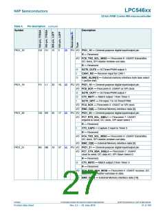
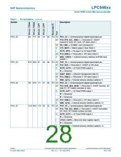
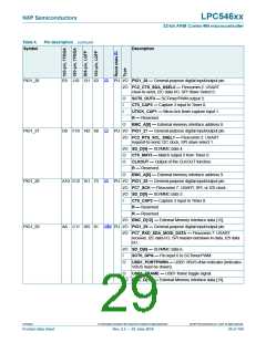
Table 4.
Symbol
Pin description …continued
Description
[2]
PIO1_22
K8 P11 89
43
PU I/O PIO1_22 — General-purpose digital input/output pin.
I/O FC8_RTS_SCL_SSEL1 — Flexcomm 8: USART
request-to-send, I2C clock, SPI slave select 1.
I/O SD_CMD — SD/MMC card command I/O.
O
I
CT2_MAT3 — Match output 3 from Timer 2.
SCT0_GPI5 — Pin input 5 to SCTimer/PWM.
I/O FC4_SSEL3 — Flexcomm 4: SPI slave select 3.
O
EMC_CKE[1] — External memory interface SDRAM clock
enable 1.
[2]
PIO1_23
K10 M10 97
46
PU I/O PIO1_23 — General-purpose digital input/output pin.
I/O FC2_SCK — Flexcomm 2: USART or SPI clock.
O
SCT0_OUT0 — SCTimer/PWM output 0.
R — Reserved.
I/O ENET_MDIO — Ethernet management data I/O.
I/O FC3_SSEL2 — Flexcomm 3: SPI slave select 2.
O
EMC_A[11] — External memory interface address 11.
[2]
PIO1_24
G8 N14 111 57
PU I/O PIO1_24 — General-purpose digital input/output pin.
I/O FC2_RXD_SDA_MOSI — Flexcomm 2: USART receiver, I2C
data I/O, SPI master-out/slave-in data.
O
SCT0_OUT1 — SCTimer/PWM output 1.
R — Reserved.
R — Reserved.
I/O FC3_SSEL3 — Flexcomm 3: SPI slave select 3.
EMC_A[12] — External memory interface address 12.
O
[2]
PIO1_25
G10 M12 119 59
PU I/O PIO1_25 — General-purpose digital input/output pin.
I/O FC2_TXD_SCL_MISO — Flexcomm 2: USART transmitter,
I2C clock, SPI master-in/slave-out data.
O
I
SCT0_OUT2 — SCTimer/PWM output 2.
R — Reserved.
UTICK_CAP0 — Micro-tick timer capture input 0.
R — Reserved.
O
EMC_A[13] — External memory interface address 13.
LPC546xx
All information provided in this document is subject to legal disclaimers.
© NXP Semiconductors N.V. 2018. All rights reserved.
Product data sheet
Rev. 2.5 — 20 June 2018
28 of 169

 NXP [ NXP ]