LPC546xx
NXP Semiconductors
32-bit ARM Cortex-M4 microcontroller
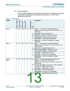
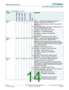
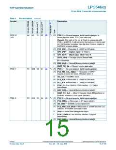
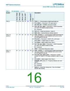
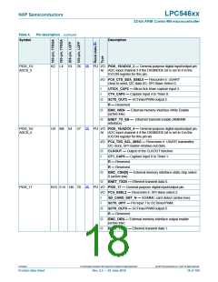
Table 4.
Symbol
Pin description …continued
Description
[2]
PIO0_3/
TCK
A6 A10 178 85
PU I/O PIO0_3 — General-purpose digital input/output pin. In
boundary scan mode: TCK (Test Clock In).
Remark: In ISP mode, this pin is set to the Flexcomm 3 SPI
MOSI function.
I/O FC3_RXD_SDA_MOSI — Flexcomm 3: USART receiver, I2C
data I/O, SPI master-out/slave-in data.
O
O
I
CT0_MAT1 — Match output 1 from Timer 0.
SCT0_OUT1 — SCTimer/PWM output 1.
SCT0_GPI3 — Pin input 3 to SCTimer/PWM.
R — Reserved.
I/O EMC_D[1] — External Memory interface data [1].
[2]
PIO0_4/
TMS
B6 C8 185 87
PU I/O PIO0_4 — General-purpose digital input/output pin. In
boundary scan mode: TMS (Test Mode Select).
Remark: The state of this pin at Reset in conjunction with
PIO0_5 and PIO0_6 will determine the boot source for the part
or if ISP handler is invoked. See the Boot Process chapter in
UM10912 for more details.
I
CAN0_RD — Receiver input for CAN 0.
I/O FC4_SCK — Flexcomm 4: USART or SPI clock.
I
I
CT3_CAP0 — Capture input 0 to Timer 3.
SCT0_GPI4 — Pin input 4 to SCTimer/PWM.
R — Reserved.
I/O EMC_D[2] — External Memory interface data [2].
ENET_MDC — Ethernet management data clock.
O
[2]
PIO0_5/
TDI
A5 E7 189 89
PU I/O PIO0_5 — General-purpose digital input/output pin.
In boundary scan mode: TDI (Test Data In).
Remark: The state of this pin at Reset in conjunction with
PIO0_4 and PIO0_6 will determine the boot source for the part
or if ISP handler is invoked. See the Boot Process chapter in
UM10912 for more details.
O
CAN0_TD — Transmitter output for CAN 0.
I/O FC4_RXD_SDA_MOSI — Flexcomm 4: USART receiver, I2C
data I/O, SPI master-out/slave-in data.
O
I
CT3_MAT0 — Match output 0 from Timer 3.
SCT0_GPI5 — Pin input 5 to SCTimer/PWM.
R — Reserved.
I/O EMC_D[3] — External Memory interface data [3].
I/O ENET_MDIO — Ethernet management data I/O.
LPC546xx
All information provided in this document is subject to legal disclaimers.
© NXP Semiconductors N.V. 2018. All rights reserved.
Product data sheet
Rev. 2.5 — 20 June 2018
14 of 169

 NXP [ NXP ]