74HC165; 74HCT165
NXP Semiconductors
8-bit parallel-in/serial out shift register
(1)
V
V
I
CP, CE input
M
GND
t
t
h
h
t
t
su
su
V
I
V
DS input
M
GND
t
su
t
V
I
W
V
CP, CE input
M
GND
mna990
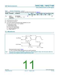
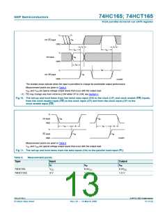
The shaded areas indicate when the input is permitted to change for predictable output performance
Measurement points are given in Table 8.
VOL and VOH are typical voltage output levels that occur with the output load.
(1) CE may change only from HIGH-to-LOW while CP is LOW, see Section 1.
Fig 10. The set-up and hold times from the serial data input (DS) to the clock (CP) and clock enable (CE) inputs,
from the clock enable input (CE) to the clock input (CP) and from the clock input (CP) to the
clock enable input (CE)
V
I
V
V
M
Dn input
GND
M
t
t
t
t
h
su
h
su
V
I
PL input
GND
V
V
M
M
mna991
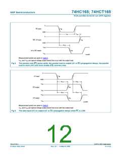
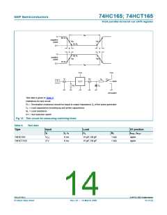
Measurement points are given in Table 8.
VOL and VOH are typical voltage output levels that occur with the output load.
Fig 11. The set-up and hold times from the data inputs (Dn) to the parallel load input (PL)
Table 8.
Type
Measurement points
Input
Output
VM
VI
VM
74HC165
VCC
3 V
0.5VCC
1.3 V
0.5VCC
1.3 V
74HCT165
74HC_HCT165_3
© NXP B.V. 2008. All rights reserved.
Product data sheet
Rev. 03 — 14 March 2008
13 of 22

 NXP [ NXP ]