74HC165; 74HCT165
NXP Semiconductors
8-bit parallel-in/serial out shift register
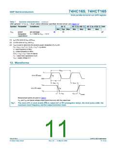
V
I
V
PL input
M
GND
t
t
rec
W
V
I
CE, CP input
V
M
GND
t
PHL
V
OH
V
Q7 or Q7 output
M
V
OL
mna988
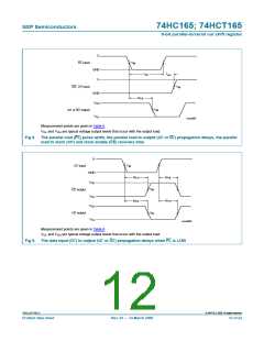
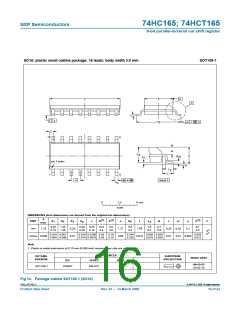
Measurement points are given in Table 8.
VOL and VOH are typical voltage output levels that occur with the output load.
Fig 8. The parallel load (PL) pulse width, the parallel load to output (Q7 or Q7) propagation delays, the parallel
load to clock (CP) and clock enable (CE) recovery time
V
I
V
D7 input
M
GND
t
t
t
t
PLH
PHL
PHL
PLH
V
OH
V
V
Q7 output
Q7 output
M
M
V
OL
V
OH
V
OL
mna989
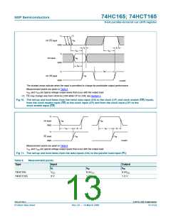
Measurement points are given in Table 8.
VOL and VOH are typical voltage output levels that occur with the output load.
Fig 9. The data input (D7) to output (Q7 or Q7) propagation delays when PL is LOW
74HC_HCT165_3
© NXP B.V. 2008. All rights reserved.
Product data sheet
Rev. 03 — 14 March 2008
12 of 22

 NXP [ NXP ]