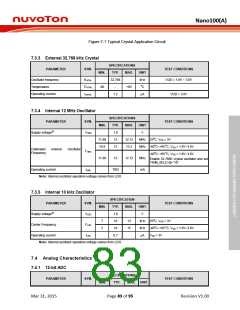
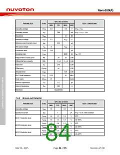
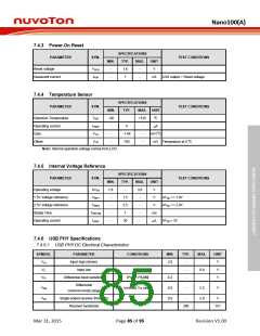
Nano100(A)
3. It is recommended that a 10uF or higher capacitor and a 100nF bypass capacitor are connected between VDD and
the closest VSS pin of the device.
4. For ensuring power stability, a 1uF or higher capacitor must be connected between LDO pin and the closest VSS pin
of the device. Also a 100nF bypass capacitor between LDO and VSS help suppressing output noise
7.3 AC Electrical Characteristics
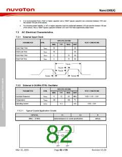
7.3.1 External Input Clock
SPECIFICATIONS
PARAMETER
SYM.
TEST CONDITIONS
MIN.
10
10
2
TYP.
MAX.
UNIT
nS
Clock High Time
tCHCX
-
-
-
-
Clock Low Time
Clock Rise Time
Clock Fall Time
tCLCX
tCLCH
tCHCL
nS
15
15
nS
2
nS
t
CLCL
t
t
CLCH
CLCX
t
t
CHCL
CHCX
7.3.2 External 4~24 MHz XTAL Oscillator
SPECIFICATIONS
PARAMETER
SYM.
TEST CONDITIONS
MIN.
4
TYP.
12
MAX.
24
UNIT
MHz
oC
Oscillator frequency
fHXTAL
THXTAL
IHXTAL
VDD = 1.8V ~ 3.6V
Temperature
-40
-
+85
Operating current
0.3
mA
VDD = 3.0V
7.3.2.1 Typical Crystal Application Circuits
CRYSTAL
C1
C2
R
4MHz ~ 24 MHz
Optional(Depend on crystal specification)
without
XT1_OUT
XT1_IN
R1
C1
C2
Mar 31, 2015
Page 82 of 95
Revision V1.00

 NUVOTON [ NUVOTON ]