Nano100(A)
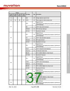
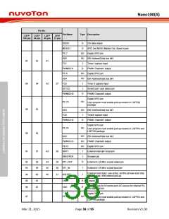
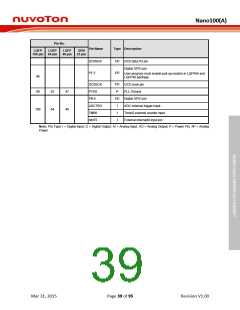
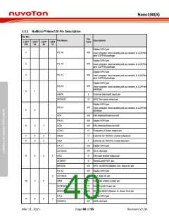
Pin No.
Pin Name
Type Description
LQFP
LQFP
LQFP
QFN
100-pin 64-pin
48-pin
33-pin
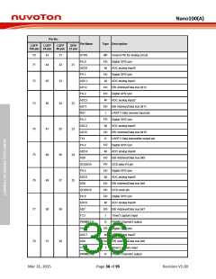
79
Vref
AP
AP
Voltage reference input for ADC
80
81
52
40
26
AVDD
Power supply for internal analog circuit
Digital GPIO pin
PD.0
I/O
User program must enable pull-up resistor in LQFP64 and
LQFP48 package.
RX1
I
UART1 Data receiver input pin
SPI2 2nd slave select pin
SmartCard1 clock pin
Digital GPIO pin
SPISS20
SC1CLK
I/O
O
PD.1
I/O
User program must enable pull-up resistor in LQFP64 and
LQFP48 package.
82
TX1
O
UART1 Data transmitter output pin
SPI2 serial clock pin
SPICLK2
SC1DAT
I/O
I/O
SmartCard1 DATA pin.
Digital GPIO pin
PD.2
I/O
User program must enable pull-up resistor in LQFP64 and
LQFP48 package.
RTSn1
O
I/O
I
UART1 Request to Send output pin
I2S left right channel clock
SPI2 1st MISO (Master In, Slave Out) pin
SmartCard1 Power pin
83
I2SLRCLK
MISO20
SC1PWR
O
Digital GPIO pin
PD.3
I/O
User program must enable pull-up resistor in LQFP64 and
LQFP48 package.
CTSn1
I
UART1 Clear to Send input pin
I2S bit clock pin
84
I2SBCLK
MOSI20
SC1RST
I/O
O
SPI2 1st MOSI (Master Out, Slave In) pin
SmartCard1 RST pin
O
Digital GPIO pin
PD.4
I/O
User program must enable pull-up resistor in LQFP64 and
LQFP48 package.
85
86
I2SDI
I
I
I
I2S data input
MISO21
SC1CD
SPI2 2nd MISO (Master In, Slave Out) pin
SmartCard1 card detect
Digital GPIO pin
PD.5
I/O
User program must enable pull-up resistor in LQFP64 and
LQFP48 package.
Mar 31, 2015
Page 37 of 95
Revision V1.00

 NUVOTON [ NUVOTON ]