M28R400CT, M28R400CB
APPENDIX B. COMMON FLASH INTERFACE (CFI)
The Common Flash Interface is a JEDEC ap-
proved, standardized data structure that can be
read from the Flash memory device. It allows a
system software to query the device to determine
various electrical and timing parameters, density
information and functions supported by the mem-
ory. The system can interface easily with the de-
vice, enabling the software to upgrade itself when
necessary.
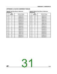
structure is read from the memory. Tables 24, 25,
26, 27, 28 and 29 show the addresses used to re-
trieve the data.
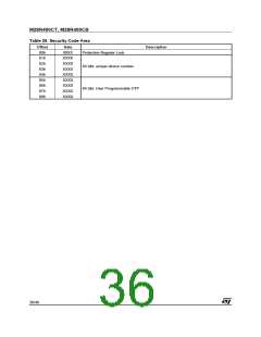
The CFI data structure also contains a security
area where a 64 bit unique security number is writ-
ten (see Table 29., Security Code Area). This area
can be accessed only in Read mode by the final
user. It is impossible to change the security num-
ber after it has been written by ST. Issue a Read
command to return to Read mode.
When the CFI Query Command (RCFI) is issued
the device enters CFI Query mode and the data
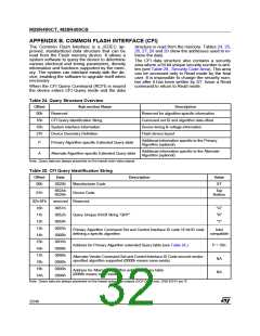
Table 24. Query Structure Overview
Offset
00h
Sub-section Name
Description
Reserved for algorithm-specific information
Command set ID and algorithm data offset
Device timing & voltage information
Flash device layout
Reserved
10h
CFI Query Identification String
System Interface Information
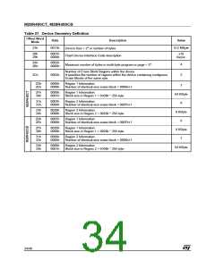
Device Geometry Definition
1Bh
27h
Additional information specific to the Primary
Algorithm (optional)
P
A
Primary Algorithm-specific Extended Query table
Alternate Algorithm-specific Extended Query table
Additional information specific to the Alternate
Algorithm (optional)
Note: Query data are always presented on the lowest order data outputs.
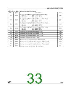
Table 25. CFI Query Identification String
Offset
Data
Description
Value
00h
0020h
Manufacturer Code
Device Code
ST
882Ah
882Bh
Top
Bottom
01h
02h-0Fh
10h
reserved Reserved
0051h
"Q"
"R"
"Y"
11h
0052h
0059h
0003h
0000h
0035h
0000h
0000h
0000h
0000h
0000h
Query Unique ASCII String "QRY"
12h
13h
Primary Algorithm Command Set and Control Interface ID code 16 bit ID code
defining a specific algorithm
Intel
compatible
14h
15h
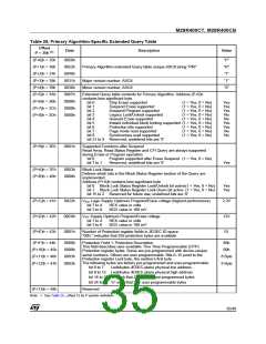
Address for Primary Algorithm extended Query table (see Table 28.)
P = 35h
NA
16h
17h
Alternate Vendor Command Set and Control Interface ID Code second vendor -
specified algorithm supported (0000h means none exists)
18h
19h
Address for Alternate Algorithm extended Query table
(0000h means none exists)
NA
1Ah
Note: Query data are always presented on the lowest order data outputs (DQ7-DQ0) only. DQ8-DQ15 are ‘0’.
32/48

 NUMONYX [ NUMONYX B.V ]