Operating features
M25P32
When Chip Select (S) is High, the device is deselected, but could remain in the Active Power
mode until all internal cycles have completed (Program, Erase, Write Status Register). The
device then goes in to the Standby Power mode. The device consumption drops to I
.
CC1
The Deep Power-down mode is entered when the specific instruction (the Deep Power-
down (DP) instruction) is executed. The device consumption drops further to I . The
CC2
device remains in this mode until another specific instruction (the Release from Deep
Power-down and Read Electronic Signature (RES) instruction) is executed.
While in the Deep Power-down mode, the device ignores all Write, Program and Erase
instructions (see Deep Power-down (DP)) This can be used as an extra software protection
mechanism, when the device is not in active use, to protect the device from inadvertent
Write, Program or Erase instructions.
4.6
4.7
Status Register
The Status Register contains a number of status and control bits that can be read or set (as
appropriate) by specific instructions. See Section 6.4: Read Status Register (RDSR) for a
detailed description of the Status Register bits.
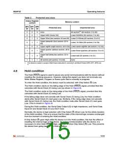
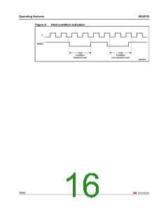
Protection modes
The environments where non-volatile memory devices are used can be very noisy. No SPI
device can operate correctly in the presence of excessive noise. To help combat this, the
M25P32 features the following data protection mechanisms:
●
Power On Reset and an internal timer (t
) can provide protection against inadvertent
PUW
changes while the power supply is outside the operating specification.
●
Program, Erase and Write Status Register instructions are checked that they consist of
a number of clock pulses that is a multiple of eight, before they are accepted for
execution.
●
All instructions that modify data must be preceded by a Write Enable (WREN)
instruction to set the Write Enable Latch (WEL) bit. This bit is returned to its reset state
by the following events:
–
–
–
–
–
–
Power-up
Write Disable (WRDI) instruction completion
Write Status Register (WRSR) instruction completion
Page Program (PP) instruction completion
Sector Erase (SE) instruction completion
Bulk Erase (BE) instruction completion
●
●
The Block Protect (BP2, BP1, BP0) bits allow part of the memory to be configured as
read-only. This is the Software Protected Mode (SPM).
The Write Protect (W/V ) signal allows the Block Protect (BP2, BP1, BP0) bits and
PP
Status Register Write Disable (SRWD) bit to be protected. This is the Hardware
Protected Mode (HPM).
●
In addition to the low power consumption feature, the Deep Power-down mode offers
extra software protection, as all Write, Program and Erase instructions are ignored.
14/53

 NUMONYX [ NUMONYX B.V ]