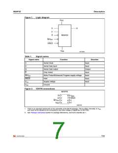
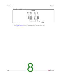
Signal description
M25P32
2.6
Write Protect/Enhanced Program supply voltage (W/VPP)
W/V is both a control input and a power supply pin. The two functions are selected by the
PP
voltage range applied to the pin.
If the W/V input is kept in a low voltage range (0 V to V ) the pin is seen as a control
PP
CC
input. This input signal is used to freeze the size of the area of memory that is protected
against program or erase instructions (as specified by the values in the BP2, BP1 and BP0
bits of the Status Register).
If V is in the range of V
it acts as an additional power supply pin. In this case V must
PP
PP
PPH
be stable until the Program/Erase algorithm is completed.
2.7
2.8
VCC supply voltage
V
is the supply voltage.
CC
VSS ground
V
is the reference for the V supply voltage.
CC
SS
10/53

 NUMONYX [ NUMONYX B.V ]