M25P32
Instructions
6.3
Read Identification (RDID)
The Read Identification (RDID) instruction allows to read the device identification data:
●
●
●
Manufacturer identification (one byte)
Device identification (two bytes)
A Unique ID code (UID) followed by 16 bytes of CFI data
The manufacturer identification is assigned by JEDEC, and has the value 20h for Numonyx.
The device identification is assigned by the device manufacturer, and indicates the memory
type in the first byte (20h), and the memory capacity of the device in the second byte (16h).
The UID is set to 10h and indicates that 16 bytes, related to the CFI content, are following.
Any Read Identification (RDID) instruction while an Erase or Program cycle is in progress, is
not decoded, and has no effect on the cycle that is in progress.
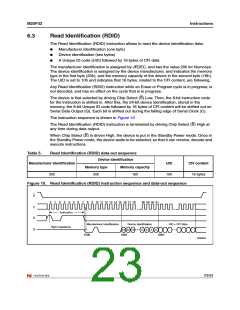
The device is first selected by driving Chip Select (S) Low. Then, the 8-bit instruction code
for the instruction is shifted in. After this, the 24-bit device identification, stored in the
memory, the 8-bit Unique ID code followed by 16 bytes of CFI content will be shifted out on
Serial Data Output (Q). Each bit is shifted out during the falling edge of Serial Clock (C).
The instruction sequence is shown in Figure 10.
The Read Identification (RDID) instruction is terminated by driving Chip Select (S) High at
any time during data output.
When Chip Select (S) is driven High, the device is put in the Standby Power mode. Once in
the Standby Power mode, the device waits to be selected, so that it can receive, decode and
execute instructions.
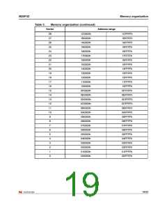
Table 5.
Read Identification (RDID) data-out sequence
Device identification
Manufacturer identification
UID
CFI content
Memory type
Memory capacity
20h
20h
16h
10h
16 bytes
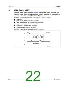
Figure 10. Read Identification (RDID) instruction sequence and data-out sequence
S
0
1
2
3
4
5
6
7
8
9
10 11 12 13 14 15
16 17 18
28 29 30 31
C
D
Instruction
Manufacturer Identification
Device Identification
UID + CFI Data
High Impedance
Q
15 14 13
MSB
3
2
1
0
MSB
MSB
AI06809c
23/53

 NUMONYX [ NUMONYX B.V ]