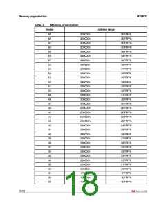
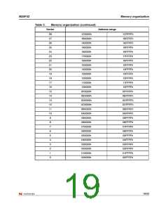
Instructions
M25P32
6.2
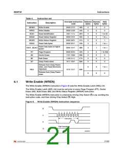
Write Disable (WRDI)
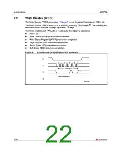
The Write Disable (WRDI) instruction (Figure 9) resets the Write Enable Latch (WEL) bit.
The Write Disable (WRDI) instruction is entered by driving Chip Select (S) Low, sending the
instruction code, and then driving Chip Select (S) High.
The Write Enable Latch (WEL) bit is reset under the following conditions:
●
Power-up
●
●
●
●
●
Write Disable (WRDI) instruction completion
Write Status Register (WRSR) instruction completion
Page Program (PP) instruction completion
Sector Erase (SE) instruction completion
Bulk Erase (BE) instruction completion
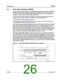
Figure 9.
Write Disable (WRDI) instruction sequence
S
0
1
2
3
4
5
6
7
C
D
Q
Instruction
High Impedance
AI03750D
22/53

 NUMONYX [ NUMONYX B.V ]