Numonyx™ Wireless Flash Memory (W18)
B.6
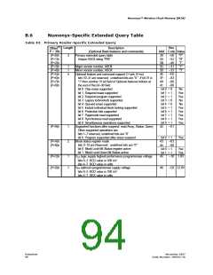
Numonyx-Specific Extended Query Table
Table 43: Primary Vendor-Specific Extended Query
Offset(1)
P = 39h
Hex
Length
Description
(Optional flash features and commands)
Primary extended query table
Add. Code Value
(P+0)h
(P+1)h
(P+2)h
(P+3)h
(P+4)h
(P+5)h
(P+6)h
(P+7)h
(P+8)h
3
39:
3A:
3B:
3C:
3D:
3E:
3F:
40:
41:
--50
--52
--49
--31
--33
--E6
--03
--00
--00
"P"
"R"
"I"
"1"
"3"
Unique ASCII string “PRI“
1
1
4
Major version number, ASCII
Minor version number, ASCII
Optional feature and command support (1=yes, 0=no)
bits 10–31 are reserved; undefined bits are “0.” If bit 31 is
“1” then another 31 bit field of Optional features follows at
the end of the bit–30 field.
bit 0 Chip erase supported
bit 1 Suspend erase supported
bit 2 Suspend program supported
bit 3 Legacy lock/unlock supported
bit 4 Queued erase supported
bit 5 Instant individual block locking supported
bit 6 Protection bits supported
bit 7 Pagemode read supported
bit 0 = 0
No
Yes
Yes
No
bit 1 = 1
bit 2 = 1
bit 3 = 0
bit 4 = 0
bit 5 = 1
bit 6 = 1
bit 7 = 1
bit 8 = 1
bit 9 = 1
No
Yes
Yes
Yes
Yes
Yes
bit 8 Synchronous read supported
bit 9 Simultaneous operations supported
Supported functions after suspend: read Array, Status, Query
Other supported operations are:
(P+9)h
1
2
42:
--01
bits 1–7 reserved; undefined bits are “0”
bit 0 Program supported after erase suspend
Block status register mask
bits 2–15 are Reserved; undefined bits are “0”
bit 0 Block Lock-Bit Status register active
bit 1 Block Lock-Down Bit Status active
bit 0 = 1
Yes
(P+A)h
(P+B)h
43:
44:
--03
--00
bit 0 = 1
bit 1 = 1
Yes
Yes
(P+C)h
(P+D)h
1
1
V
CC logic supply highest performance program/erase voltage
45:
--18 1.8V
bits 0–3 BCD value in 100 mV
bits 4–7 BCD value in volts
VPP optimum program/erase supply voltage
46:
--C0 12.0V
bits 0–3 BCD value in 100 mV
bits 4–7 HEX value in volts
Datasheet
94
November 2007
Order Number: 290701-18

 NUMONYX [ NUMONYX B.V ]