Numonyx™ Wireless Flash Memory (W18)
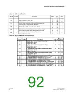
Table 40: CFI Identification
Hex
Code
Offset
Length
Description
Addr.
Value
10:
11:
12:
--51
--52
--59
“Q”
“R”
“Y”
10h
3
Query-unique ASCII string “QRY”
Primary vendor command set and control interface ID code.
16-bit ID code for vendor-specific algorithms.
13:
14:
--03
--00
13h
15h
17h
19h
2
2
2
2
—
—
—
—
15:
16:
--39
--00
Extended Query Table primary algorithm address
Alternate vendor command set and control interface ID code.
0000h means no second vendor-specified algorithm exists.
17:
18:
--00
--00
Secondary algorithm Extended Query Table address.
0000h means none exists.
19:
1A:
--00
--00
Table 41: System Interface Information
Hex
Code
Offset
Length
Description
Add.
Value
1Bh
1
VCC logic supply minimum program/erase voltage
bits 0–3 BCD 100 mV
bits 4–7 BCD volts
1B:
--17 1.7V
--19 1.9V
--B4 11.4V
--C6 12.6V
--04 16μs
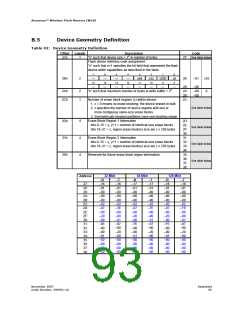
1Ch
1Dh
1Eh
1
1
1
V
V
V
CC logic supply maximum program/erase voltage
1C:
1D:
1E:
bits 0–3 BCD 100 mV
bits 4–7 BCD volts
PP [programming] supply minimum program/erase voltage
bits 0–3 BCD 100 mV
bits 4–7 HEX volts
PP [programming] supply maximum program/erase voltage
bits 0–3 BCD 100 mV
bits 4–7 HEX volts
“n” such that typical single word program time-out = 2n μ-sec
“n” such that typical max. buffer write time-out = 2n μ-sec
“n” such that typical block erase time-out = 2n m-sec
1Fh
20h
21h
22h
23h
24h
25h
26h
1
1
1
1
1
1
1
1
1F:
20:
21:
22:
23:
24:
25:
26:
--00
--0A
--00
NA
1s
NA
“n” such that typical full chip erase time-out = 2n m-sec
“n” such that maximum word program time-out = 2n times typical
“n” such that maximum buffer write time-out = 2n times typical
“n” such that maximum block erase time-out = 2n times typical
“n” such that maximum chip erase time-out = 2n times typical
--04 256μs
--00
--03
--00
NA
8s
NA
Datasheet
92
November 2007
Order Number: 290701-18

 NUMONYX [ NUMONYX B.V ]