M29FxxxFT, M29FxxxFB
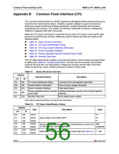
Common Flash Interface (CFI)
Value
Address
Data
Description
x16
x8
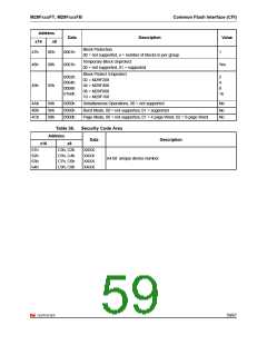
17h
2Eh
0000h
0000h
0000h
0000h
Alternate Vendor Command Set and Control Interface ID Code
second vendor - specified algorithm supported
NA
NA
18h
19h
1Ah
30h
32h
34h
Address for Alternate Algorithm extended Query table
Query data are always presented on the lowest order data outputs (DQ7-DQ0) only. DQ8-DQ15 are ‘0’.
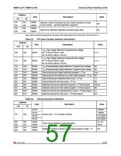
Table 33. CFI Query System Interface Information
Address
x16 x8
Data
Description
Value
VCC Logic Supply Minimum Program/Erase voltage
bit 7 to 4BCD value in volts
1Bh
1Ch
36h
38h
0045h
4.5 V
bit 3 to 0BCD value in 100 mV
VCC Logic Supply Maximum Program/Erase voltage
0055h
bit 7 to 4BCD value in volts
5.5 V
bit 3 to 0BCD value in 100 mV
1Dh
1Eh
1Fh
20h
21h
22h
23h
24h
25h
26h
3Ah
3Ch
3Eh
40h
42h
44h
46h
48h
4Ah
4Ch
0000h
0000h
0003h
0000h
000Ah
0000h
0004h
0000h
0003h
0000h
VPP [Programming] Supply Minimum Program/Erase voltage
VPP [Programming] Supply Maximum Program/Erase voltage
Typical timeout per single Byte/Word program = 2n µs
Typical timeout for minimum size write buffer program = 2n µs NA
Typical timeout per individual block erase = 2n ms
Typical timeout for full chip erase = 2n ms
Maximum timeout for Byte/Word program = 2n times typical
Maximum timeout for write buffer program = 2n times typical
Maximum timeout per individual block erase = 2n times typical 8 s
Maximum timeout for chip erase = 2n times typical
NA
NA
NA
8 µs
1 s
NA
256 µs
NA
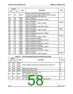
Table 34.
Device Geometry Definition
Data
0015h
Address
Description
Value
x16
x8
2 MByte
0014h
0013h
0012h
1 MByte
27h
4Eh
Device Size = 2n in number of Bytes
512 KByte
256 KByte
28h
29h
50h
52h
0002h
0000h
x8, x16
Async.
Flash Device Interface Code description
2Ah
2Bh
54h
56h
0000h
0000h
Maximum number of Bytes in multi-Byte program or page = 2n
NA
57/67

 NUMONYX [ NUMONYX B.V ]