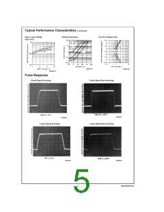
Pulse Response (Continued)
=
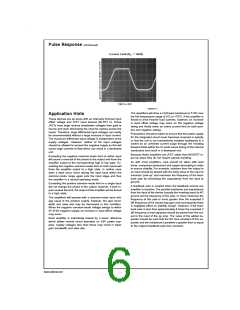
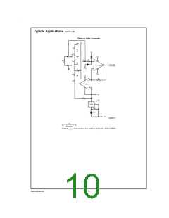
Current Limit (RL 100Ω)
DS008357-10
±
The amplifiers will drive a 2 kΩ load resistance to 10V over
the full temperature range of 0˚C to +70˚C. If the amplifier is
forced to drive heavier load currents, however, an increase
in input offset voltage may occur on the negative voltage
swing and finally reach an active current limit on both posi-
tive and negative swings.
Application Hints
These devices are op amps with an internally trimmed input
offset voltage and JFET input devices (BI-FET II). These
JFETs have large reverse breakdown voltages from gate to
source and drain eliminating the need for clamps across the
inputs. Therefore, large differential input voltages can easily
be accommodated without a large increase in input current.
The maximum differential input voltage is independent of the
supply voltages. However, neither of the input voltages
should be allowed to exceed the negative supply as this will
cause large currents to flow which can result in a destroyed
unit.
Precautions should be taken to ensure that the power supply
for the integrated circuit never becomes reversed in polarity
or that the unit is not inadvertently installed backwards in a
socket as an unlimited current surge through the resulting
forward diode within the IC could cause fusing of the internal
conductors and result in a destroyed unit.
Because these amplifiers are JFET rather than MOSFET in-
put op amps they do not require special handling.
Exceeding the negative common-mode limit on either input
will cause a reversal of the phase to the output and force the
amplifier output to the corresponding high or low state. Ex-
ceeding the negative common-mode limit on both inputs will
force the amplifier output to a high state. In neither case
does a latch occur since raising the input back within the
common-mode range again puts the input stage and thus
the amplifier in a normal operating mode.
As with most amplifiers, care should be taken with lead
dress, component placement and supply decoupling in order
to ensure stability. For example, resistors from the output to
an input should be placed with the body close to the input to
minimize “pick-up” and maximize the frequency of the feed-
back pole by minimizing the capacitance from the input to
ground.
Exceeding the positive common-mode limit on a single input
will not change the phase of the output; however, if both in-
puts exceed the limit, the output of the amplifier will be forced
to a high state.
A feedback pole is created when the feedback around any
amplifier is resistive. The parallel resistance and capacitance
from the input of the device (usually the inverting input) to AC
ground set the frequency of the pole. In many instances the
frequency of this pole is much greater than the expected 3
dB frequency of the closed loop gain and consequently there
is negligible effect on stability margin. However, if the feed-
back pole is less than approximately 6 times the expected 3
dB frequency a lead capacitor should be placed from the out-
put to the input of the op amp. The value of the added ca-
pacitor should be such that the RC time constant of this ca-
pacitor and the resistance it parallels is greater than or equal
to the original feedback pole time constant.
The amplifiers will operate with a common-mode input volt-
age equal to the positive supply; however, the gain band-
width and slew rate may be decreased in this condition.
When the negative common-mode voltage swings to within
3V of the negative supply, an increase in input offset voltage
may occur.
Each amplifier is individually biased by a zener reference
which allows normal circuit operation on 6V power sup-
plies. Supply voltages less than these may result in lower
gain bandwidth and slew rate.
±
www.national.com
6

 NSC [ National Semiconductor ]