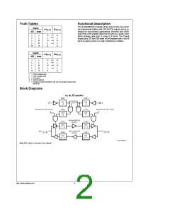
Description of BOUNDARY-SCAN Circuitry
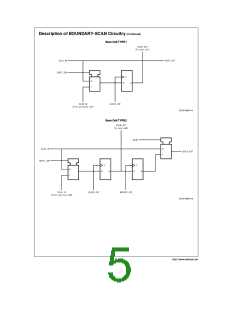
The scan cells used in the BOUNDARY-SCAN register are
one of the following two types depending upon their loca-
tion. Scan cell TYPE1 is intended to solely observe system
data, while TYPE2 has the additional ability to control sys-
tem data. (See IEEE Standard 1149.1 Figure 10-11 for a
further description of scan cell TYPE1 and Figure 10-12 for
a further description of scan cell TYPE2.)
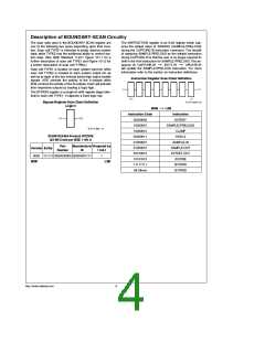
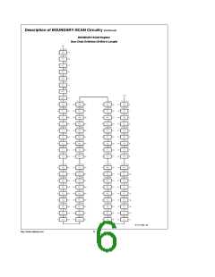
The INSTRUCTION register is an 8-bit register which cap-
tures the default value of 10000001 (SAMPLE/PRELOAD)
during the CAPTURE-IR instruction command. The benefit
of capturing SAMPLE/PRELOAD as the default instruction
during CAPTURE-IR is that the user is no longer required to
qshuieftnicnethoef:8C-bAitPinTsUtrRuEct-iIoRn xfor SAMPLE/PRELOAD. The se-
EXIT1-IR
x
UPDATE-IR
will update the SAMPLE/PRELOAD instruction. For more
information refer to the section on instruction definitions.
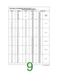
Scan cell TYPE1 is located on each system input pin while
scan cell TYPE2 is located at each system output pin as
well as at each of the two internal active-high output enable
signals. AOE controls the activity of the A-outputs while
BOE controls the activity of the B-outputs. Each will activate
their respective outputs by loading a logic high.
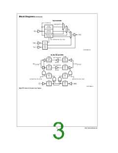
Instruction Register Scan Chain Definition
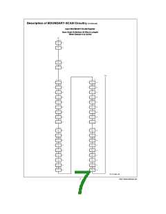
The BYPASS register is a single bit shift register stage iden-
tical to scan cell TYPE1. It captures a fixed logic low.
Bypass Register Scan Chain Definition
Logic 0
TL/F/11657–10
MSB
Instruction Code
x
LSB
Instruction
00000000
10000001
10000010
00000011
01000001
01000010
00100010
10101010
11111111
All Others
EXTEST
SAMPLE/PRELOAD
CLAMP
TL/F/11657–17
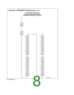
SCAN182245A Product IDCODE
(32-Bit Code per IEEE 1149.1)
HIGH-Z
SAMPLE-IN
SAMPLE-OUT
EXTEST-OUT
IDCODE
Part
Manufacturer Required by
Version Entity
Number
ID
1149.1
0000 111111 0000000000 00000001111
MSB
1
LSB
BYPASS
BYPASS
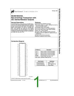
http://www.national.com
4

 NSC [ National Semiconductor ]