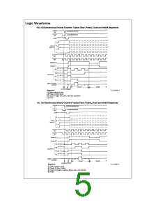
Absolute Maximum Ratings (Notes 1 & 2)
If Military/Aerospace specified devices are required,
please contact the National Semiconductor Sales
Office/Distributors for availability and specifications.
Operating Conditions
Min
Max
Units
Supply Voltage (V
)
2
0
6
V
CC
DC Input or Output Voltage
(V , V
V
CC
V
b
a
0.5 to 7.0V
Supply Voltage (V
)
CC
)
IN OUT
b
b
a
a
DC Input Voltage (V
)
1.5 to V
1.5V
0.5V
IN
CC
CC
Operating Temp. Range (T )
A
DC Output Voltage (V
)
0.5 to V
b
b
a
85
a
125
MM74HC
MM54HC
40
55
C
OUT
§
C
g
g
g
Clamp Diode Current (I , I
)
20 mA
25 mA
50 mA
§
IK OK
DC Output Current, per pin (I
)
Input Rise or Fall Times
OUT
e
e
e
(t , t )
r f
V
V
V
2.0V
4.5V
6.0V
1000
500
ns
ns
ns
DC V or GND Current, per pin (I
CC
)
CC
CC
CC
CC
b
a
65 C to 150 C
Storage Temperature Range (T
)
§
§
STG
400
Power Dissipation (P )
D
(Note 3)
600 mW
500 mW
S.O. Package only
Lead Temp. (T ) (Soldering 10 seconds)
L
260 C
§
DC Electrical Characteristics (Note 4)
74HC
eb
54HC
e
T
A
25 C
§
eb
A
T
A
40 to 85 C
§
T
55 to 125 C
§
Symbol
Parameter
Conditions
V
CC
Units
Typ
Guaranteed Limits
V
V
V
Minimum High Level
Input Voltage
2.0V
4.5V
6.0V
1.5
3.15
4.2
1.5
3.15
4.2
1.5
3.15
4.2
V
V
V
IH
Maximum Low Level
2.0V
4.5V
6.0V
0.5
1.35
1.8
0.5
1.35
1.8
0.5
1.35
1.8
V
V
V
IL
Input Voltage**
e
V or V
IH IL
Minimum High Level
Output Voltage
V
I
OH
IN
s
20 mA
2.0V
4.5V
6.0V
2.0
4.5
6.0
1.9
4.4
5.9
1.9
4.4
5.9
1.9
4.4
5.9
V
V
V
l
OUT
l
e
V
I
V
or V
IH IL
IN
s
s
4.0 mA
5.2 mA
4.5V
6.0V
4.2
5.7
3.98
5.48
3.84
5.34
3.7
5.2
V
V
l
l
OUT
OUT
l
l
I
e
V or V
IH IL
V
OL
Maximum Low Level
Output Voltage
V
IN
s
I
20 mA
2.0V
4.5V
6.0V
0
0
0
0.1
0.1
0.1
0.1
0.1
0.1
0.1
0.1
0.1
V
V
V
l
OUT
l
e
V
I
V
or V
IH IL
IN
s
s
4.0 mA
5.2 mA
4.5V
6.0V
0.2
0.2
0.26
0.26
0.33
0.33
0.4
0.4
V
V
l
l
OUT
OUT
l
l
I
e
g
g
g
1.0
I
I
Maximum Input
Current
V
V
or GND 6.0V
0.1
1.0
mA
IN
IN
CC
e
Maximum Quiescent
Supply Current
V
IN
V
CC
or GND 6.0V
8.0
80
160
mA
CC
e
I
0 mA
OUT
Note 1: Absolute Maximum Ratings are those values beyond which damage to the device may occur.
Note 2: Unless otherwise specified all voltages are referenced to ground.
b
b
Note 3: Power Dissipation temperature derating Ð plastic ‘‘N’’ package: 12 mW/ C from 65 C to 85 C; ceramic ‘‘J’’ package: 12 mW/ C from 100 C to 125 C.
§
§
§
§
Note 4: For a power supply of 5V 10% the worst case output voltages (V , and V ) occur for HC at 4.5V. Thus the 4.5V values should be used when designing
§
§
g
OH OL
5.5V and 4.5V respectively. (The V value at 5.5V is 3.85V.) The worst case leakage current (I , I , and
IH IN CC
e
with this supply. Worst case V and V occur at V
IH IL
CC
) occur for CMOS at the higher voltage and so the 6.0V values should be used.
I
OZ
**V limits are currently tested at 20% of V . The above V specification (30% of V ) will be implemented no later than Q1, CY’89.
IL CC IL CC
2

 NSC [ National Semiconductor ]