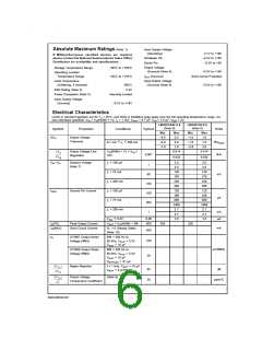
Electrical Characteristics (Continued)
Limits in standard typeface are for TJ = 25˚C, and limits in boldface type apply over the full operating temperature range. Un-
less otherwise specified: VIN = VO(NOM) + 1V, IL = 1 mA, COUT = 4.7 µF, CIN = 2.2 µF, VS/D = 2V.
LM2987/8AI-X.X
LM2987/8I-X.X
(Note 6)
(Note 6)
Symbol
IDELAY
Parameter
Conditions
Typical
Units
Min
1.6
1.4
Max
2.8
Min
1.6
1.4
Max
2.8
Delay Pin Current
Source
2.2
µA
3.0
3.0
SHUTDOWN INPUT
VS/D S/D Input Voltage
VH = O/P ON
1.4
0.55
0
1.6
1.6
V
(Note 8)
VL = O/P OFF
VS/D = 0
0.18
−1
0.18
−1
IS/D
S/D Input Current
µA
VS/D = 5V
5
15
15
ERROR COMPARATOR
IOH
Output “HIGH” Leakage
VOH = 16V
1
1
0.01
150
µA
2
2
VOL
Output “LOW” Voltage
VIN = VO(NOM) − 0.5V,
IO(COMP) = 300 µA
220
350
−3.5
−2.5
−4.9
−3.3
220
350
−3.5
−2.5
−4.9
−3.3
mV
VTHR
(MAX)
Upper Threshold
Voltage
−5.5
−7.7
−5.5
−7.7
−4.6
VTHR
(MIN)
Lower Threshold
Voltage
−8.9
−8.9
%VOUT
−6.6
2.0
−13.0
−13.0
HYST
Hysteresis
Note 1: Absolute Maximum Ratings indicate limits beyond which damage to the component may occur. Electrical specifications do not apply when operating the de-
vice outside of its rated operating conditions.
Note 2: The ESD rating of the Bypass pin is 500V (LP2988 only.)
Note 3: The maximum allowable power dissipation is a function of the maximum junction temperature, T (MAX), the junction-to-ambient thermal resistance, θ
,
J−A
J
and the ambient temperature, T . The maximum allowable power dissipation at any ambient temperature is calculated using:
A
The value of θ
for the SO-8 (M) package is 160˚C/W, and the mini SO-8 (MM) package is 200˚C/W. Exceeding the maximum allowable power dissipation will cause
J−A
excessive die temperature, and the regulator will go into thermal shutdown.
Note 4: If used in a dual-supply system where the regulator load is returned to a negative supply, the LM2987/8 output must be diode-clamped to ground.
Note 5: The output PNP structure contains a diode between the V and V
IN
terminals that is normally reverse-biased. Forcing the output above the input will turn
OUT
on this diode and may induce a latch-up mode which can damage the part (see Application Hints).
Note 6: Limits are 100% production tested at 25˚C. Limits over the operating temperature range are guaranteed through correlation using Statistical Quality Control
(SQC) methods. The limits are used to calculate National’s Average Outgoing Quality Level (AOQL).
Note 7: Dropout voltage is defined as the input to output differential at which the output voltage drops 100 mV below the value measured with a 1V differential.
Note 8: To prevent mis-operation, the Shutdown input must be driven by a signal that swings above V and below V with a slew rate not less than 40 mV/µs (see
H
L
Application Hints).
Note 9: Temperature coefficient is defined as the maximum (worst-case) change divided by the total temperature range.
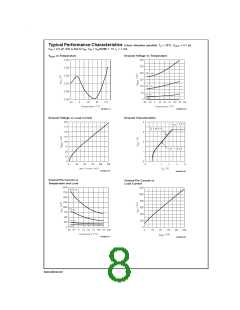
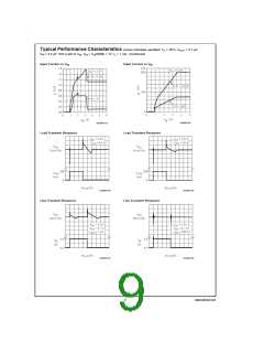
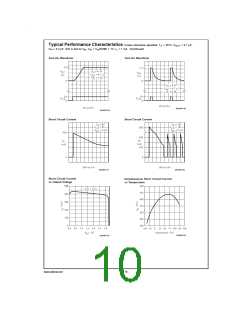
Note 10: See Typical Performance Characteristics curves.
7
www.national.com

 NSC [ National Semiconductor ]