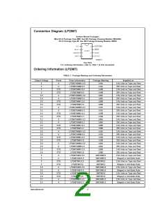
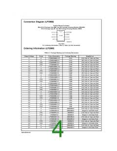
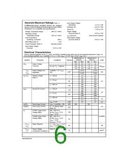
Absolute Maximum Ratings (Note 1)
If Military/Aerospace specified devices are required,
please contact the National Semiconductor Sales Office/
Distributors for availability and specifications.
Input Supply Voltage
(Operating)
2.1V to +16V
−0.3V to +16V
−0.3V to +6V
Shutdown Pin
Sense Pin
Output Voltage
Storage Temperature Range
−65˚C to +150˚C
(Survival) (Note 4)
−0.3V to +16V
Operating Junction
Temperature Range
I
OUT (Survival)
Short Circuit Protected
−40˚C to +125˚C
Input-Output Voltage
(Survival) (Note 5)
Lead Temperature
(Soldering, 5 seconds)
−0.3V to +16V
260˚C
2 kV
ESD Rating (Note 2)
Power Dissipation (Note 3)
Internally Limited
Input Supply Voltage
(Survival)
−0.3V to +16V
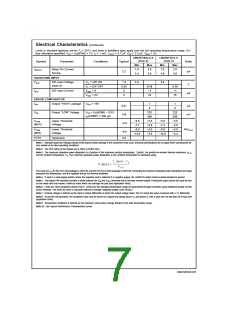
Electrical Characteristics
Limits in standard typeface are for TJ = 25˚C, and limits in boldface type apply over the full operating temperature range. Un-
less otherwise specified: VIN = VO(NOM) + 1V, IL = 1 mA, COUT = 4.7 µF, CIN = 2.2 µF, VS/D = 2V.
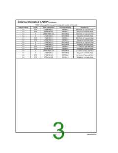
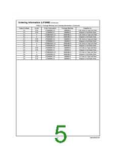
LM2987/8AI-X.X
LM2987/8I-X.X
(Note 6)
(Note 6)
Symbol
∆VO
Parameter
Conditions
Typical
Units
Min
−0.5
−0.8
−1.8
Max
0.5
Min
−1.0
−1.6
−2.8
Max
1.0
Output Voltage
Tolerance
<
<
0.1 mA IL 200 mA
0.8
1.6
%VNOM
%/V
1.8
2.8
Output Voltage Line
Regulation
VO(NOM) + 1V ≤ VIN
≤
0.014
0.014
0.007
16V
0.032
0.032
VIN–VO
Dropout Voltage
(Note 7)
IL = 100 µA
IL = 75 mA
IL = 200 mA
IL = 100 µA
IL = 75 mA
IL = 200 mA
2.0
3.5
2.0
3.5
1
120
170
230
350
120
150
800
1400
2.1
120
170
230
350
120
150
800
1400
2.1
90
mV
µA
180
100
500
1
IGND
Ground Pin Current
mA
µA
3.7
3.7
<
VS/D 0.3V
0.05
400
1.5
1.5
I
O(PK)
Peak Output Current
Short Circuit Current
VOUT ≥ VO(NOM) − 5%
250
250
mA
IO(MAX)
RL = 0 (Steady State)
(Note 10)
400
en
LP2987 Output Noise
Voltage (RMS)
BW = 300 Hz to
50 kHz, VOUT = 3.3V
COUT = 10 µF
100
µV(RMS)
LP2988 Output Noise
Voltage (RMS)
BW = 300 Hz to
50 kHz, VOUT = 3.3V
COUT = 10 µF
20
CBYPASS = .01 µF
Ripple Rejection
f = 1 kHz, COUT = 10 µF
65
20
dB
=
CBYP 0 (LP2988)
Output Voltage
Temperature Coefficient
(Note 9)
ppm/˚C
www.national.com
6

 NSC [ National Semiconductor ]