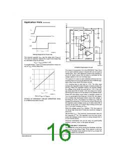
Care must be taken to ensure that the capacitor selected for
bypass will not have significant leakage current over the op-
erating temperature range of the application.
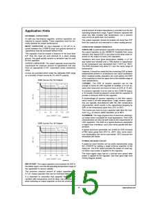
Application Hints (Continued)
To assure proper operation, the signal source used to drive
the Shutdown input must be able to swing above and below
the specified turn-on/turn-off voltage thresholds listed as VH
and VL, respectively (see Electrical Characteristics).
A high quality ceramic capacitor which uses either NPO or
COG type dielectiric material will typically have very low
leakage. Small surface-mount polypropolene or polycarbon-
ate film capacitors also have extremely low leakage, but are
slightly larger in size than ceramics.
It is also important that the turn-on (and turn-off) voltage sig-
nals applied to the Shutdown input have a slew rate which is
not less than 40 mV/µs.
CAUTION: the regulator output state can not be guaranteed
if a slow-moving AC (or DC) signal is applied that is in the
range between VH and VL.
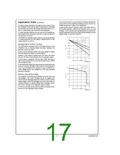
REVERSE INPUT-OUTPUT VOLTAGE
The PNP power transistor used as the pass element in the
LP2987/8 has an inherent diode connected between the
regulator output and input.
During normal operation (where the input voltage is higher
than the output) this diode is reverse-biased.
However, if the output is pulled above the input, this diode
will turn ON and current will flow into the regulator output.
In such cases, a parasitic SCR can latch which will allow a
high current to flow into VIN (and out the ground pin), which
can damage the part.
DS100017-49
In any application where the output may be pulled above the
input, an external Schottky diode must be connected from
V
IN to VOUT (cathode on VIN, anode on VOUT), to limit the re-
verse voltage across the LP2987/8 to 0.3V (see Absolute
Maximum Ratings).
BYPASS CAPACITOR (LP2988)
The capacitor connected to the Bypass pin must have very
low leakage. The current flowing out of the Bypass pin
comes from the Bandgap reference, which is used to set the
output voltage. Since the Bandgap circuit has only a few mi-
croamps flowing in it, loading effects due to leakage current
will cause a change in the regulated output voltage.
Curves are provided which show the effect of loading the By-
pass pin on the regulated output voltage.
DS100017-50
17
www.national.com

 NSC [ National Semiconductor ]