Application Hints (Continued)
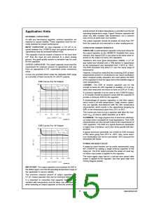
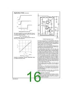
DS100017-9
Timing Diagram for Power-Up
The external capacitor cDLY sets the delay time (TDELAY).
The value of capacitor required for a given time delay may
be calculated using the formula:
CDLY = TDELAY/(5.59 X 105)
To simplify design, a plot is provided below which shows val-
ues of CDLY versus delay time.
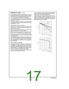
DS100017-10
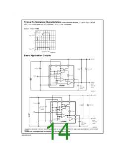
LP2987/8 Equivalent Circuit
The output of comparator U2 is the ERR/RESET flag. Since
it is an open-collector output, it requires the use of a pull-up
resistor (RP). The 1.23V reference is tied to the inverting in-
put of U2, which means that its output is controlled by the
voltage applied to the non-inverting input.
The output of U1 (also an open-collector) will force the non-
inverting input of U2 to go low whenever the LP2987/8 regu-
lated output drops about 5% below nominal.
U1’s inverting input is also held at 1.23V. The other input
samples the regulated output through a resistive divider (RA
and RB). When the regulated output is at nominal voltage,
the voltage at the divider tap point will be 1.23V. If this volt-
age drops about 60 mV below 1.23V, the output of U1 will go
low forcing the output of U2 low (which is the ERROR state).
DS100017-11
Power-ON reset delay occurs when a capacitor (shown as
Plot of CDLY vs TDELAY
C
DLY) is connected to the Delay pin. At turn-ON, this capaci-
tor is initially fully discharged (which means the voltage at
the Delay pin is 0V). The output of U1 keeps CDLY fully dis-
charged (by sinking the 2.2 µA from the current source) until
the regulator output voltage comes up to within about 5% of
nominal. At this point, U1’s output stops sinking current and
DETAILS OF ERR/RESET CIRCUIT OPERATION: (Refer
to LP2987/8 Equivalent Circuit).
the 2.2 µA starts charging up CDLY
.
When the voltage across CDLY reaches 1.23V, the output of
U2 will go high (note that D1 limits the maximum voltage to
about 2V).
SELECTING CDLY: The maximum recommended value for
this capacitor is 1 µF. The capacitor must not have exces-
sively high leakage current, since it is being charged from a
2.2 µA current source.
Aluminum electrolytics can not be used, but good-quality
tantalum, ceremic, mica, or film types will work.
SHUTDOWN INPUT OPERATION
The LP2987/8 is shut off by driving the Shutdown input low,
and turned on by pulling it high. If this feature is not to be
used, the Shutdown input should be tied to VIN to keep the
regulator output on at all times.
www.national.com
16

 NSC [ National Semiconductor ]