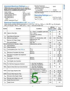
Mounting Temperature
ꢁInfrared or Convection (20 sec.)
Thermal Resistance
Absolute Maximum Ratings (Note 1)
If Military/Aerospace specified devices are required,
please contact the National Semiconductor Sales Office/
Distributors for availability and specifications.
235°C
70°C/W
ꢀθJA (microSMD)
Soldering Information See AN-1112 “microSMD Wafer Level
Chip Scale Package.”
Supply Voltage
6.0V
Storage Temperature
Power Dissipation (Note 3)
ESD Rating (Note 4)
ESD Rating (Note 5)
CDM
-85°C to +150°C
Internally Limited
2000V
200V
500V
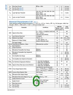
Operating Ratings (Note 1)
Supply Voltage
2.7V ≤ VDD ≤ 5.5V
TMIN ≤ TA ≤ TMAX
−40°C ≤TA ≤+85°C
Junction Temperature (TJMAX
)
150°C
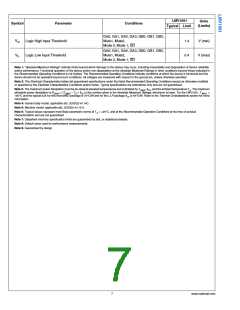
Electrical Characteristics 3.3V (Note 1, Note 2)
Unless otherwise specified, all limits guaranteed for TA = 25°C, VDD = 3.3V, VIN = 18mVP-P, f = 1kHz, SD = VDD, Pre Amp gain =
20dB, Post Amp gain = 6dB, RL = 100kΩ, and CL = 4.7pF, f = 1kHz pass through mode.
LMV1091
Units
Symbol
Parameter
Conditions
Typical Limits
(Limits)
(Note 6) (Note 7)
VIN = 18mVP-P, A-weighted, Audio band
63
65
5
dB
SNR Signal-to-Noise Ratio
VOUT = 18VP-P
,
dB
voice band (300–3400Hz)
A-Weighted
eN
Input Referred Noise level
Maximum Input Signal
μVRMS
VIN
mVP-P (min)
THD+N < 1%, Pre Amp Gain = 6dB
Differential Out+, Out-
THD+N < 1%
880
820
1.1
VRMS (min)
Maximum AC Output Voltage
DC Level at Outputs
1.2
VOUT
Out+, Out-
820
0.1
mV
% (max)
kΩ
THD+N Total Harmonic Distortion + Noise
Differential Out+ and Out-
0.2
ZIN
Input Impedance
142
220
ZOUT
Output Impedance
Ω
RLOAD
CLOAD
10
100
kΩ (min)
pF (max)
ZLOAD
AM
Load Impedance (Out+, Out-) (Note 9)
Minimum
Maximum
6
36
dB
dB
Microphone Preamplifier Gain Range
Microphone Preamplifier Gain Adjustment
Resolution
1.7
2.3
dB (min)
dB (max)
AMR
2
Minimum
Maximum
6
18
dB
dB
AP
Post Amplifier Gain Range
2.6
3.4
dB (min)
dB (max)
APR
Post Amplifier Gain Resolution
3
f = 1kHz (See Test Method)
f = 300Hz (See Test Method)
34
42
26
FFNSE
SNRIE
Far Field Noise Suppression Electrical
Signal-to-Noise Ratio Improvement Electrical
dB
dB
f = 1kHz (See Test Method)
f = 300Hz (See Test Method)
26
33
18
Input Referred, Input AC grounded
fRIPPLE = 217Hz (VRIPPLE = 100mVP-P
)
99
95
60
85
80
dB (min)
dB (min)
dB
PSRR Power Supply Rejection Ratio
CMRR Common Mode Rejection Ratio
fRIPPLE = 1kHz (VRIPPLE = 100mVP-P
)
Input referred
1.85
2.15
V (min)
V (max)
VBM
IBIAS = 1.2mA
Microphone Bias Supply Voltage
2.0
A-Weighted, CB = 10nF
VIN = 0V
7
eVBM Mic bias noise voltage on VREF pin
IDDQ Supply Quiescent Current
μVRMS
0.60
0.8
mA (max)
VIN = 25mVP-P both inputs
Noise cancelling mode
IDD
Supply Current
0.60
mA
5
www.national.com

 NSC [ National Semiconductor ]