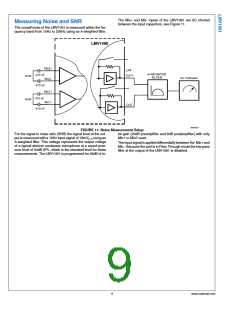
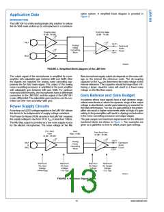
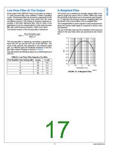
cation system. A simplified block diagram is provided in
Figure 3.
Application Data
INTRODUCTION
The LMV1091 is a fully analog single chip solution to reduce
the far field noise picked up by microphones in a communi-
30092224
FIGURE 3. Simplified Block Diagram of the LMV1091
The output signal of the microphones is amplified by a pre-
amplifier with adjustable gain between 6dB and 36dB. After
the signals are matched the analog noise cancelling sup-
presses the far field noise signal. The output of the analog
noise cancelling processor is amplified in the post amplifier
with adjustable gain between 6dB and 18dB. For optimum
noise and EMI immunity, the microphones have a differential
connection to the LMV1091 and the output of the LMV1091
is also differential. The adjustable gain functions can be con-
trolled via GA0–GA3 and GB0–GB2 pins.
Bias microphone supply output pin depends on the noise volt-
age on the internal the reference node. The de-coupling
capacitor on the VREF pin determines the noise voltage on this
internal reference. This capacitor should be larger than 1nF;
having a larger capacitor value will result in a lower noise
voltage on the Mic Bias output.
Gain Balance and Gain Budget
In systems where input signals have a high dynamic range,
critical noise levels or where the dynamic range of the output
voltage is also limited, careful gain balancing is essential for
the best performance. Too low of a gain setting in the pream-
plifier can result in higher noise levels while too high of a gain
setting in the preamplifier will result in clipping and saturation
in the noise cancelling processor and output stages.
Power Supply Circuits
A low drop-out (LDO) voltage regulator in the LMV1091 allows
the device to be independent of supply voltage variations.
The Power On Reset (POR) circuitry in the LMV1091 requires
the supply voltage to rise from 0V to VDD in less than 100ms.
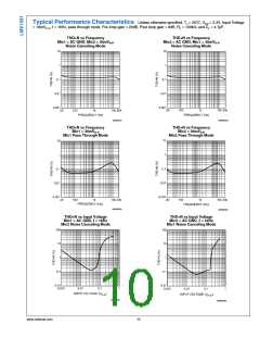
The gain ranges and maximum signal levels for the different
functional blocks are shown in Figure 4. Two examples are
given as a guideline on how to select proper gain settings.
The Mic Bias output is provided as a low noise supply source
for the electret microphones. The noise voltage on the Mic
30092241
FIGURE 4. Maximum Signal Levels
13
www.national.com

 NSC [ National Semiconductor ]