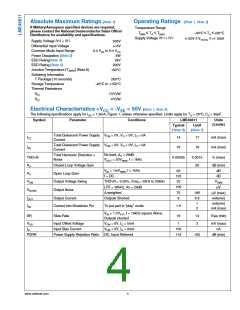
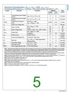
Electrical Characteristics +VCC = –VEE = 100V (Note 1, Note 2)
The following specifications apply for ISD = 1.5mA, Figure 1, unless otherwise specified. Limits apply for TA = 25°C.
Symbol
Parameter
Conditions
LME49811
Units
(Limits)
Typical
Limit
(Note 6)
(Note 7)
Total Quiescent Power Supply
Current
ICC
IEE
VCM = 0V, VO = 0V, IO = 0A
VCM = 0V, VO = 0V, IO = 0A
17
22
24
mA (max)
mA (max)
% (max)
Total Quiescent Power Supply
Current
19
Total Harmonic Distortion +
Noise
No load, AV = 30dB
THD+N
AV
0.00035
0.001
26
VOUT = 30VRMS, f = 1kHz
Closed Loop Voltage Gain
dB (min)
dB
VIN = 1mVRMS, f = 1kHz
f = DC
93
120
68
AV
Open Loop Gain
dB
VOM
Output Voltage Swing
THD+N = 0.05%, Freq = 20Hz to 20kHz
LPF = 30kHz, Av = 29dB
A-weighted
VRMS
100
70
μV
VNOISE
Output Noise
180
7
μV (max)
mA(min)
IOUT
ISD
Output Current
Outputs Shorted
9
1
2
mA(min)
mA (max)
Current into Shutdown Pin
To put part in “play” mode
1.5
17
VIN = 1.2VP-P, f = 10kHz square Wave,
Outputs shorted
SR
Slew Rate
14
3
V/μs (min)
VOS
IB
Input Offset Voltage
Input Bias Current
VCM = 0V, IO = 0mA
1
mV (max)
nA (max)
dB (min)
VCM = 0V, IO = 0mA
100
115
PSRR
Power Supply Rejection Ratio f = DC, Input Referred
105
Note 1: “Absolute Maximum Ratings” indicate limits beyond which damage to the device may occur, including inoperability and degradation of device reliability
and/or performance. Functional operation of the device and/or non-degradation at the Absolute Maximum Ratings or other conditions beyond those indicated in
the Recommended Operating Conditions is not implied. The Recommended Operating Conditions indicate conditions at which the device is functional and the
device should not be operated beyond such conditions. All voltages are measured with respect to the ground pin, unless otherwise specified
Note 2: The Electrical Characteristics tables list guaranteed specifications under the listed Recommended Operating Conditions except as otherwise modified
or specified by the Electrical Characteristics Conditions and/or Notes. Typical specifications are estimations only and are not guaranteed.
Note 3: The maximum power dissipation must be derated at elevated temperatures and is dictated by TJMAX, θJA, and the ambient temperature, TA. The maximum
allowable power dissipation is PDMAX = (TJMAX - TA) / θJA or the number given in Absolute Maximum Ratings, whichever is lower.
Note 4: Human body model, applicable std. JESD22-A114C.
Note 5: Machine model, applicable std. JESD22-A115-A.
Note 6: Typical values represent most likely parametric norms at TA = +25ºC, and at the Recommended Operation Conditions at the time of product
characterization and are not guaranteed.
Note 7: Datasheet min/max specification limits are guaranteed by test or statistical analysis.
Note 8: The maximum operating junction temperature is 150°C.
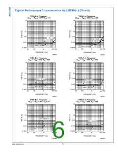
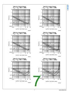
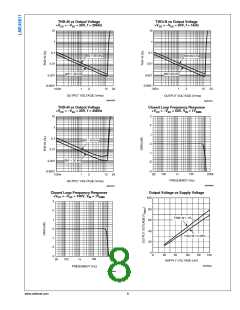
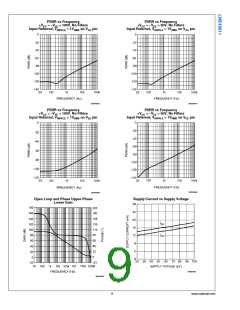
Note 9: The Data taken with Bandwidth = 30kHz, AV = 29dB, CC = 30pF, and TA = 25°C except where specified.
5
www.national.com

 NSC [ National Semiconductor ]