Absolute Maximum Ratings (Note 1)
Operating Ratings (Note 1, Note 2)
If Military/Aerospace specified devices are required,
please contact the National Semiconductor Sales Office/
Distributors for availability and specifications.
Temperature Range
TMIN ≤ TA ≤ TMAX
−40°C ≤TA ≤+85°C
+/-20V ≤VTOTAL ≤+/-100V
Supply Voltage |V+| + |V-|
Supply Voltage |V+| + |V-|
Differential Input Voltage
Common Mode Input Range
Power Dissipation (Note 3)
ESD Rating(Note 4)
200V
+/-6V
0.4 VEE to 0.4 VCC
4W
2kV
ESD Rating (Note 5)
200V
150°C
Junction Temperature (TJMAX) (Note 8)
Soldering Information
T Package (10 seconds)
Storage Temperature
Thermal Resistance
260°C
-40°C to +150°C
ꢁθJA
73°C/W
4°C/W
ꢁθJC
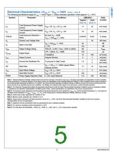
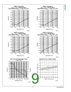
Electrical Characteristics +VCC = -VEE = 50V (Note 1, Note 2)
The following specifications apply for ISD = 1.5mA, Figure 1, unless otherwise specified. Limits apply for TA = 25°C, CC = 30pF.
Symbol
Parameter
Conditions
LME49811
Units
(Limits)
Typical
Limit
(Note 6)
(Note 7)
Total Quiescent Power Supply VCM = 0V, VO = 0V, IO = 0A
Current
ICC
IEE
14
17
19
mA (max)
mA (max)
% (max)
Total Quiescent Power Supply VCM = 0V, VO = 0V, IO = 0A
Current
16
No load, AV = 29dB
Total Harmonic Distortion +
Noise
THD+N
AV
0.00055
0.0015
26
VOUT = 20VRMS, f = 1kHz
Closed Loop Voltage Gain
dB (min)
dB
VIN = 1mVRMS, f = 1kHz
f = DC
93
120
33
AV
Open Loop Gain
dB
VOM
Output Voltage Swing
THD+N = 0.05%, Freq = 20Hz to 20kHz
LPF = 30kHz, Av = 29dB
A-weighted
VRMS
100
μV
VNOISE
Output Noise
70
8
180
6.5
μV (max)
mA(min)
IOUT
ISD
Output Current
Outputs Shorted
1
2
mA(min)
mA (max)
Current into Shutdown Pin
To put part in “play” mode
1.5
16
VIN = 1.2VP-P, f = 10kHz square Wave,
Outputs shorted
SR
Slew Rate
13
3
V/μs (min)
VOS
IB
Input Offset Voltage
Input Bias Current
VCM = 0V, IO = 0mA
1
mV (max)
nA
VCM = 0V, IO = 0mA
100
115
PSRR
Power Supply Rejection Ratio DC, Input Referred
105
dB (min)
www.national.com
4

 NSC [ National Semiconductor ]