With large values of RIN oscillations may be observed on the
outputs when the inputs are left floating. Decreasing the value
of RIN or not letting the inputs float will remove the oscillations.
If the value of RIN is decreased then the value of CIN will need
to increase in order to maintain the same -3dB frequency re-
sponse.
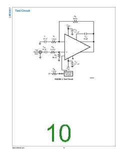
signed output stage, combine with a VBE multiplier, can elim-
inate the trim pot and virtually eliminate crossover distortion.
The VCE voltage of QMULT (also called BIAS of the output
stage) can be set by following formula:
VBIAS = VBE(1+RB2/RB1) ꢀ (V)
(6)
COMPENSATION CAPACITOR
The compensation capacitor (CC) is one of the most critical
external components in value, placement and type. The ca-
pacitor should be placed close to the LME49811 and a silver
mica type will give good performance. The value of the ca-
pacitor will affect slew rate and stability. The highest slew rate
is possible while also maintaining stability through out the
power and frequency range of operation results in the best
audio performance. The value shown in Figure 1 should be
considered a starting value with optimization done on the
bench and in listening testing.
When using a bipolar output stage with the LME49811 (as in
Figure 1), the designer must beware of thermal runaway.
Thermal runaway is a result of the temperature dependence
of VBE (an inherent property of the transistor). As temperature
increases, VBE decreases. In practice, current flowing through
a bipolar transistor heats up the transistor, which lowers the
VBE. This in turn increases the current gain, and the cycle re-
peats. If the system is not designed properly this positive
feedback mechanism can destroy the bipolar transistors used
in the output stage. One of the recommended methods of
preventing thermal runaway is to use the same heat sink on
the bipolar output stage transistor together with VBE multiplier
transistor. When the VBE multiplier transistor is mounted to the
same heat sink as the bipolar output stage transistors, it tem-
perature will track that of the output transistors. Its VBE is
dependent upon temperature as well, and so it will draw more
current as the output transistors heat up, reducing the bias
voltage to compensate. This will limit the base current into the
output transistors, which counteracts thermal runaway. An-
other widely popular method of preventing thermal runaway
is to use low value emitter degeneration resistors (RE1 and
RE2). As current increases, the voltage at the emitter also in-
creases, which decreases the voltage across the base and
emitter. This mechanism helps to limit the current and coun-
teracts thermal runaway.
SUPPLY BYPASSING
The LME49811 has excellent power supply rejection and
does not require a regulated supply. However, to eliminate
possible oscillations all op amps and power op amps should
have their supply leads bypassed with low-inductance capac-
itors having short leads and located close to the package
terminals. Inadequate power supply bypassing will manifest
itself by a low frequency oscillation known as “motorboating”
or by high frequency instabilities. These instabilities can be
eliminated through multiple bypassing utilizing a large elec-
trolytic capacitor (10μF or larger) which is used to absorb low
frequency variations and a small ceramic capacitor (0.1μF) to
prevent any high frequency feedback through the power sup-
ply lines. If adequate bypassing is not provided the current in
the supply leads which is a rectified component of the load
current may be fed back into internal circuitry. This signal
causes low distortion at high frequencies requiring that the
supplies be bypassed at the package terminals with an elec-
trolytic capacitor of 470μF or more.
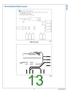
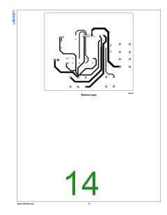
LAYOUT CONSIDERATION AND AVOIDING GROUND
LOOPS
A proper layout is virtually essential for a high performance
audio amplifier. It is very important to return the load ground,
supply grounds of output transistors, and the low level (feed-
back and input) grounds to the circuit board common ground
point through separate paths. When ground is routed in this
fashion, it is called a star ground or a single point ground. It
is advisable to keep the supply decoupling capacitors of
0.1μF close as possible to LME49811 to reduce the effects of
PCB trace resistance and inductance. Following the general
rules will optimize the PCB layout and avoid ground loops
problems:
OUTPUT STAGE USING BIPOLAR TRANSISTORS
With a properly designed output stage and supply voltage of
±100V, an output power up to 500W can be generated at
0.05% THD+N into an 8Ω speaker load. With an output cur-
rent of several amperes, the output transistors need substan-
tial base current drive because power transistors usually have
quite low current gain—typical hfe of 50 or so. To increase the
current gain, audio amplifiers commonly use Darlington style
devices or additional driver stages. Power transistors should
be mounted together with the VBE multiplier transistor on the
same heat sink to avoid thermal run away. Please see the
section Biasing Technique and Avoiding Thermal Run-
away for additional information.
a) Make use of symmetrical placement of components.
b) Make high current traces, such as output path traces, as
wide as possible to accommodate output stage current re-
quirement.
c) To reduce the PCB trace resistance and inductance, same
ground returns paths should be as short as possible. If pos-
sible, make the output traces short and equal in length.
BIASING TECHNIQUES AND AVOIDING THERMAL
RUNAWAY
A class AB amplifier has some amount of distortion called
Crossover distortion. To effectively minimize the crossover
distortion from the output, a VBE multiplier may be used in-
stead of two biasing diodes. A VBE multiplier normally consists
of a bipolar transistor (QMULT, see Figure 1) and two resistors
(RB1 and RB2, see Figure 1). A trim pot can also be added in
series with RB1 for optional bias adjustment. A properly de-
d) To reduce the PCB trace resistance and inductance,
ground returns paths should be as short as possible.
e) If possible, star ground or a single point ground should be
observed. Advanced planning before starting the PCB can
improve audio performance.
www.national.com
12

 NSC [ National Semiconductor ]