Application Information
SHUTDOWN FUNCTION
thermal compound, the thermal resistance, θCS (case to sink),
is about 0.2°C/W. Since convection heat flow (power dissi-
pation) is analogous to current flow, thermal resistance is
analogous to electrical resistance, and temperature drops are
analogous to voltage drops, the power dissipation out of the
LME49811 is equal to the following:
The shutdown function of the LME49811 is controlled by the
amount of current that flows into the shutdown pin. If there is
less than 1mA of current flowing into the shutdown pin, the
part will be in shutdown. This can be achieved by shorting the
shutdown pin to ground or by floating the shutdown pin. If
there is between 1mA and 2mA of current flowing into the
shutdown pin, the part will be in “play” mode. This can be done
by connecting a reference voltage to the shutdown pin
through a resistor (RM). The current into the shutdown pin can
be determined by the equation ISD = (VREF – 2.9) / RM. For
example, if a 5V power supply is connected through a
1.4kΩ resistor to the shutdown pin, then the shutdown current
will be 1.5mA, at the center of the specified range. It is also
possible to use VCC as the power supply for the shutdown pin,
though RM will have to be recalculated accordingly. It is not
recommended to flow more than 2mA of current into the shut-
down pin because damage to the LME49811 may occur.
PDMAX = (TJMAX−TAMB) / θJA
(1)
where TJMAX = 150°C, TAMB is the system ambient tempera-
ture and θJA = θJC + θCS + θSA
.
It is highly recommended to switch between shutdown and
“play” modes rapidly. This is accomplished most easily
through using a toggle switch that alternatively connects the
shutdown pin through a resistor to either ground or the shut-
down pin power supply. Slowly increasing the shutdown cur-
rent may result in undesired voltages on the outputs of the
LME49811, which can damage an attached speaker.
30004855
Once the maximum package power dissipation has been cal-
culated using equation 1, the maximum thermal resistance,
SA, (heat sink to ambient) in °C/W for a heat sink can be
calculated. This calculation is made using equation 2 which
is derived by solving for θSA in equation 1.
θ
θ
SA = [(TJMAX−TAMB)−PDMAX(θJC +θCS)] / PDMAX
(2)
THERMAL PROTECTION
The LME49811 has a thermal protection scheme to prevent
long-term thermal stress of the device. When the temperature
on the die exceeds 150°C, the LME49811 shuts down. It
starts operating again when the die temperature drops to
about 145°C, but if the temperature again begins to rise, shut-
down will occur again above 150°C. Therefore, the device is
allowed to heat up to a relatively high temperature if the fault
condition is temporary, but a sustained fault will cause the
device to cycle in a Schmitt Trigger fashion between the ther-
mal shutdown temperature limits of 150°C and 145°C. This
greatly reduces the stress imposed on the IC by thermal cy-
cling, which in turn improves its reliability under sustained
fault conditions.
Again it must be noted that the value of θSA is dependent upon
the system designer's amplifier requirements. If the ambient
temperature that the audio amplifier is to be working under is
higher than 25°C, then the thermal resistance for the heat
sink, given all other things are equal, will need to be smaller.
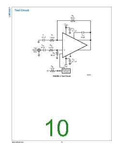
PROPER SELECTION OF EXTERNAL COMPONENTS
Proper selection of external components is required to meet
the design targets of an application. The choice of external
component values that will affect gain and low frequency re-
sponse are discussed below.
The gain of each amplifier is set by resistors RF and Ri for the
non-inverting configuration shown in Figure 1. The gain is
found by Equation 3 below:
Since the die temperature is directly dependent upon the heat
sink used, the heat sink should be chosen so that thermal
shutdown is not activated during normal operation. Using the
best heat sink possible within the cost and space constraints
of the system will improve the long-term reliability of any pow-
er semiconductor device, as discussed in the Determining
the Correct Heat Sink section.
AV = RF / Riꢀ (V/V)
(3)
For best noise performance, lower values of resistors are
used. A value of 1kΩ is commonly used for Ri and then setting
the value of RF for the desired gain. For the LME49811 the
gain should be set no lower than 26dB. Gain settings below
26dB may experience instability.
POWER DISSIPATION AND HEAT SINKING
When in “play” mode, the LME49811 draws a constant
amount of current, regardless of the input signal amplitude.
Consequently, the power dissipation is constant for a given
supply voltage and can be computed with the equation
PDMAX = ICC* (VCC– VEE).
The combination of Ri with Ci (see Figure 1) creates a high
pass filter. The low frequency response is determined by
these two components. The -3dB point can be found from
Equation 4 shown below:
fi = 1 / (2πRiCi)ꢀ (Hz)
(4)
DETERMINING THE CORRECT HEAT SINK
If an input coupling capacitor is used to block DC from the
inputs as shown in Figure 5, there will be another high pass
filter created with the combination of CIN and RIN. When using
a input coupling capacitor RIN is needed to set the DC bias
point on the amplifier's input terminal. The resulting -3dB fre-
quency response due to the combination of CIN and RIN can
be found from Equation 5 shown below:
The choice of a heat sink for a high-power audio amplifier is
made entirely to keep the die temperature at a level such that
the thermal protection circuitry is not activated under normal
circumstances.
The thermal resistance from the die to the outside air, θJA
(junction to ambient), is a combination of three thermal resis-
tances, θJC (junction to case), θCS (case to sink), and θSA (sink
to ambient). The thermal resistance, θJC (junction to case), of
the LME49811 is 0.4 °C/W. Using Thermalloy Thermacote
fIN = 1 / (2πRINCIN)ꢀ (Hz)
(5)
11
www.national.com

 NSC [ National Semiconductor ]