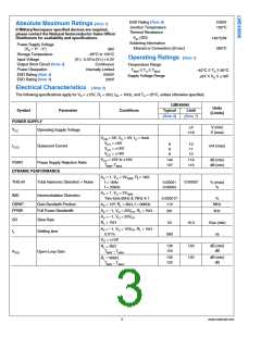
LME49990
Units
(Limits)
Symbol
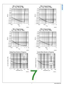
NOISE
Parameter
Conditions
Typical
Limit
(Note 6)
(Note 7)
f = 10Hz
f = 100Hz
f = 1kHz
f = 10kHz
1.4
1.0
ꢀnV/√Hz
ꢀnV/√Hz
ꢀnV/√Hz (max)
eN
Input Noise Voltage Density
0.88
0.88
1.3
ꢀnV/√Hz
nVPP
BW = 0.1Hz to 10Hz (Note 4)
BW = 10Hz to 20kHz
BW = 10Hz to 1MHz
30
0.12
1
V_NOISE
iN
RMS Voltage Noise
μV (max)
μV (max)
0.2
1.2
Input Current Noise Density
f = 1kHz
2.8
ꢀpA/√Hz
INPUT CHARACTERISTICS
VCC = ±18V, VCM = 0v, VO = 0V
VCC = ±18V, TMIN − TMAX
μV (max)
μV (max)
130
300
1000
2000
VOS
Offset Voltage
Input Offset Voltage Drift vs
VOS Drift
IBIAS
VCC = ±18V, TMIN − TMAX
2
μV/°C
Temperature (ΔVOS/ΔTemp)
VCC = ±18V, VCM = 0v, VO = 0V
VCC = ±18V, TMIN − T MAX
30
150
500
1000
nA (max)
nA (max)
Input Bias Current
VCC = ±18V, VCM = 0v, VO = 0V
VCC = ±18V, TMIN − TMAX
35
95
400
1000
nA (max)
nA (max)
IOS
Input Offset Current
VIN-CM
CMRR
Common-Mode Input Voltage Range
Common-Mode Rejection
12
11
V (min)
–10V<VCM<10V
TMIN − TMAX
137
132
118
110
dB (min)
dB (min)
OUTPUT CHARACTERISTICS
VCC = ±15V, RL = 2kΩ
VCC = ±15V, RL = 600Ω
VCC = ±18V, RL = 600Ω
VCC = ±18V
±13
±13
±16
12.5
12
14.0
V (min)
V (min)
V (min)
VOUT
Output Voltage Swing
ISHIRT
IOUT
Output Short-Circuit Current
Output Current
+75/-70
26
+55/-50
24
mA (min)
mA (min)
VCC = ±18V, RL = 600Ω
Note 1: “Absolute Maximum Ratings” indicate limits beyond which damage to the device may occur, including inoperability and degradation of device reliability
and/or performance. Functional operation of the device and/or non-degradation at the Absolute Maximum Ratings or other conditions beyond those indicated in
the Recommended Operating Conditions is not implied. The Recommended Operating Conditions indicate conditions at which the device is functional and the
device should not be operated beyond such conditions. All voltages are measured with respect to the ground pin, unless otherwise specified.
Note 2: The Electrical Characteristics tables list guaranteed specifications under the listed Recommended Operating Conditions except as otherwise modified
or specified by the Electrical Characteristics Conditions and/or Notes. Typical specifications are estimations only and are not guaranteed.
Note 3: Amplifier output connected to GND, any number of amplifiers within a package.
Note 4: Human body model, applicable std. JESD22-A114C.
Note 5: Machine model, applicable std. JESD22-A115-A.
Note 6: Typical values represent most likely parametric norms at TA = +25ºC, and at the Recommended Operation Conditions at the time of product
characterization and are not guaranteed.
Note 7: Datasheet min/max specification limits are guaranteed by test or statistical analysis.
Note 8: Charge device model, applicable std JESD22–C101–A.
www.national.com
4

 NSC [ National Semiconductor ]