Functional Description
DS012893-15
1.0 PIN DESCRIPTION
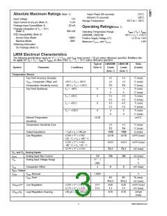
V+
This is the positive supply voltage pin. This pin
should be bypassed with 0.1 µF capacitor to
ground.
GND
VREF
This is the ground pin.
This is the 1.250V bandgap voltage reference out-
put pin. In order to maintain trip point accuracy this
pin should source a 50 µA load.
VTEMP This is the temperature sensor output pin.
OUT1
This is an open collector digital output. OUT1 is ac-
tive LOW. It goes LOW when the temperature is
greater than T1 and goes HIGH when the tempera-
ture drops below T1–5˚C. This output is not in-
tended to directly drive a fan motor.
OUT2
This is an open collector digital output. OUT2 is ac-
tive LOW. It goes LOW when the temperature is
greater than the T2 set point and goes HIGH when
the temperature is less than T2–5˚C. This output is
not intended to directly drive a fan motor.
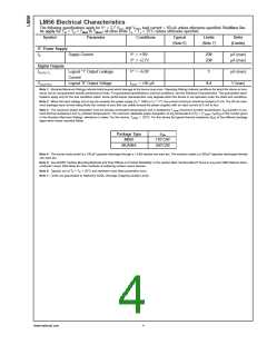
DS012893-16
V
V
= 1.250V x (R1)/(R1 + R2 + R3)
= 1.250V x (R1 + R2)/(R1 + R2 + R3)
T1
T2
where:
(R1 + R2 + R3) = 27 kΩ and
VT1
VT2
This is the input pin for the temperature trip point
voltage for OUT1.
V
= [6.20 mV/˚C x T] + 395 mV therefore:
T1 or T2
R1 = V /(1.25V) x 27 kΩ
T1
This is the input pin for the low temperature trip
point voltage for OUT2.
R2 = (V /(1.25V) x 27 k)Ω–R1
T2
R3 = 27 kΩ − R1 − R2
7
www.national.com

 NSC [ National Semiconductor ]