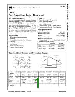
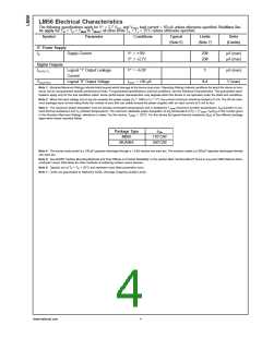
LM56 Electrical Characteristics
The following specifications apply for V+ = 2.7 VDC, and VREF load current = 50 µA unless otherwise specified. Boldface lim-
its apply for TA = TJ = TMIN to TMAX; all other limits TA = TJ = 25˚C unless otherwise specified.
Symbol
Parameter
Conditions
Typical
Limits
Units
(Note 6)
(Note 7)
(Limits)
V+ Power Supply
IS
Supply Current
V+ = +10V
230
230
µA (max)
µA (max)
V+ = +2.7V
V+ = +5.0V
IOUT = +50 µA
Digital Outputs
IOUT(“1”)
Logical “1” Output Leakage
Current
1
µA (max)
V (max)
VOUT(“0”)
Logical “0” Output Voltage
0.4
Note 1: Absolute Maximum Ratings indicate limits beyond which damage to the device may occur. Operating Ratings indicate conditions for which the device is func-
tional, but do not guarantee specific performance limits. For guaranteed specifications and test conditions, see the Electrical Characteristics. The guaranteed speci-
fications apply only for the test conditions listed. Some performance characteristics may degrade when the device is not operated under the listed test conditions.
+
<
>
V ), the current at that pin should be limited to 5 mA. The 20 mA maxi-
Note 2: When the input voltage (V ) at any pin exceeds the power supply (V
GND or V
I
I
I
mum package input current rating limits the number of pins that can safely exceed the power supplies with an input current of 5 mA to four.
Note 3: The maximum power dissipation must be derated at elevated temperatures and is dictated by T (maximum junction temperature), θ (junction to am-
Jmax
JA
bient thermal resistance) and T (ambient temperature). The maximum allowable power dissipation at any temperature is P = (T
–T )/θ or the number given
A JA
A
D
Jmax
in the Absolute Maximum Ratings, whichever is lower. For this device, T
= 125˚C. For this device the typical thermal resistance (θ ) of the different package
JA
Jmax
types when board mounted follow:
Package Type
M08A
θJA
110˚C/W
250˚C/W
MUA08A
Note 4: The human body model is a 100 pF capacitor discharge through a 1.5 kΩ resistor into each pin. The machine model is a 200 pF capacitor discharged directly
into each pin.
Note 5: See AN450 “Surface Mounting Methods and Their Effects on Product Reliability” or the section titled “Surface Mount” found in any post 1986 National Semi-
conductor Linear Data Book for other methods of soldering surface mount devices.
Note 6: Typicals are at T = T = 25˚C and represent most likely parametric norm.
J
A
Note 7: Limits are guaranteed to National’s AOQL (Average Outgoing Quality Level).
www.national.com
4

 NSC [ National Semiconductor ]