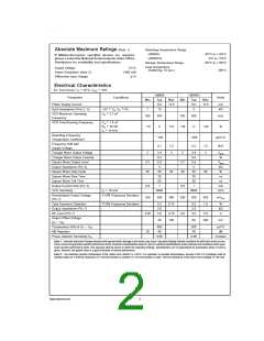
Absolute Maximum Ratings (Note 1)
If Military/Aerospace specified devices are required,
please contact the National Semiconductor Sales Office/
Distributors for availability and specifications.
Operating Temperature Range
LM565H
−55˚C to +125˚C
0˚C to +70˚C
LM565CN
Storage Temperature Range
−65˚C to +150˚C
Lead Temperature
(Soldering, 10 sec.)
±
Supply Voltage
12V
260˚C
Power Dissipation (Note 2)
Differential Input Voltage
1400 mW
±
1V
Electrical Characteristics
=
=
±
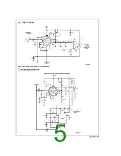
AC Test Circuit, TA 25˚C, VCC
6V
LM565
LM565C
Typ
8.0
Parameter
Conditions
Units
Max
Min
Typ
8.0
10
Max
Min
Power Supply Current
12.5
12.5
mA
<
<
Input Impedance (Pins 2, 3)
−4V V2, V3 0V
7
5
kΩ
=
Co 2.7 pF
VCO Maximum Operating
Frequency
300
500
250
−30
500
kHz
=
Co 1.5 nF
VCO Free-Running Frequency
=
Ro 20 kΩ
−10
0
+10
0
+30
%
=
fo 10 kHz
Operating Frequency
Temperature Coefficient
−100
0.1
−200
0.2
ppm/˚C
%/V
Frequency Drift with
Supply Voltage
1.0
3
1.5
3
Triangle Wave Output Voltage
Triangle Wave Output Linearity
Square Wave Output Level
Output Impedance (Pin 4)
Square Wave Duty Cycle
Square Wave Rise Time
Square Wave Fall Time
Output Current Sink (Pin 4)
VCO Sensitivity
2
2.4
0.2
5.4
5
2
2.4
0.5
5.4
5
Vp-p
%
4.7
45
4.7
40
Vp-p
kΩ
50
55
50
60
%
20
20
ns
50
50
ns
0.6
1
0.6
1
mA
Hz/V
=
fo 10 kHz
6600
6600
±
Demodulated Output Voltage
(Pin 7)
10% Frequency Deviation
250
300
400
200
300
450
1.5
mVp-p
±
Total Harmonic Distortion
Output Impedance (Pin 7)
DC Level (Pin 7)
10% Frequency Deviation
0.2
3.5
4.5
0.75
0.2
3.5
4.5
%
kΩ
V
4.25
4.75
100
4.0
5.0
Output Offset Voltage
|V7 − V6|
30
50
200
mV
Temperature Drift of |V7 − V6|
AM Rejection
500
40
500
40
µV/˚C
dB
30
Phase Detector Sensitivity KD
0.68
0.68
V/radian
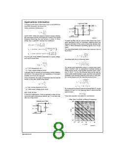
Note 1: Absolute Maximum Ratings indicate limits beyond which damage to the device may occur. Operating Ratings indicate conditions for which the device is func-
tional, but do not guarantee specific performance limits. Electrical Characteristics state DC and AC electrical specifications under particular test conditions which guar-
antee specific performance limits. This assumes that the device is within the Operating Ratings. Specifications are not guaranteed for parameters where no limit is
given, however, the typical value is a good indication of device performance.
Note 2: The maximum junction temperature of the LM565 and LM565C is +150˚C. For operation at elevated temperatures, devices in the TO-5 package must be
derated based on a thermal resistance of +150˚C/W junction to ambient or +45˚C/W junction to case. Thermal resistance of the dual-in-line package is +85˚C/W.
www.national.com
2

 NSC [ National Semiconductor ]