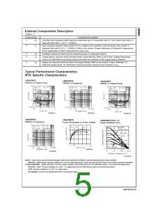
Electrical Characteristics for Bridged-Mode Operation (Notes 3, 4) (Continued)
=
=
The following specifications apply for VDD 5V unless otherwise specified. Limits apply for TA 25˚C.
Symbol
Parameter
Conditions
LM4863
Units
(Limits)
Typical
Limit
(Note
13)
(Note
14)
=
=
XTALK
SNR
Channel Separation
f
1 kHz, CB 1.0 µF
90
98
dB
dB
=
VDD 5V, PO = 1.1W, RL = 8Ω
Signal To Noise Ratio
Electrical Characteristics for Single-Ended Operation (Notes 3, 4)
=
=
The following specifications apply for VDD 5V unless otherwise specified. Limits apply for TA 25˚C.
Symbol
Parameter
Conditions
LM4863
Units
(Limits)
Typical
Limit
(Note
13)
(Note
14)
=
VOS
PO
Output Offset Voltage
Output Power
VIN 0V
5
50
75
mV (max)
mW (min)
mW
=
=
=
THD 0.5%, f 1 kHz, RL 32Ω
85
=
=
=
THD+N 1%, f 1 kHz, RL 8Ω
340
440
0.2
=
=
=
THD+N 10%, f 1 kHz, RL 8Ω
mW
=
=
THD+N Total Harmonic Distortion+Noise AV −1, PO 75 mW, 20 Hz ≤ f ≤ 20 kHz,
%
=
RL 32Ω
=
=
PSRR
Power Supply Rejection Ratio
CB 1.0 µF, VRIPPLE 200 mV
,
52
dB
RMS
=
f
1 kHz
1 kHz, CB 1.0 µF
=
=
XTALK
SNR
Channel Separation
f
60
95
dB
dB
=
VDD 5V, PO = 340mW, RL = 8Ω
Signal To Noise Ratio
Note 3: All voltages are measured with respect to the ground pins, 2, 7, and 15, unless otherwise specified.
Note 4: Absolute Maximum Ratings indicate limits beyond which damage to the device may occur. Operating Ratings indicate conditions for which the device is func-
tional, but do not guarantee specific performance limits. Electrical Characteristics state DC and AC electrical specifications under particular test conditions which guar-
antee specific performance limits. This assumes that the device is within the Operating Ratings. Specifications are not guaranteed for parameters where no limit is
given, however, the typical value is a good indication of device performance.
2
Note 5: The θ given is for an MXA20A package whose exposed-DAP is soldered to an exposed 2in piece of 1 ounce printed circuit board copper.
JA
Note 6: The θ given is for an MXA20A package whose exposed-DAP is not soldered to any copper.
JA
Note 7: When driving 3Ω loads from a 5V supply, the LM4863MTE must be mounted to the circuit board and forced-air cooled (450 linear-feet per minute).
Note 8: When driving 4Ω loads from a 5V supply, the LM4863MTE must be mounted to the circuit board.
Note 9: Output power is measured at the device terminals.
Note 10: The maximum power dissipation must be derated at elevated temperatures and is dictated by T
JMAX
, θ , and the ambient temperature T . The maximum
JA
A
=
=
150˚C. For the θ s for different packages, please see the Application Informa-
JA
allowable power dissipation is P
(T
− T )/θ . For the LM4863, T
JA JMAX
DMAX
JMAX
A
tion section or the Absolute Maximum Ratings section.
Note 11: Human body model, 100 pF discharged through a 1.5 kΩ resistor.
Note 12: Machine model, 220 pF–240 pF discharged through all pins.
Note 13: Typicals are measured at 25˚C and represent the parametric norm.
Note 14: Limits are guaranteed to National’s AOQL (Average Outgoing Quality Level).
Note 15: The quiescent power supply current depends on the offset voltage when a practical load is connected to the amplifier.
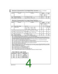
Truth Table for Logic Inputs
SHUTDOWN
HP-IN
LM4863 MODE
Low
Low
Bridged
Low
High
Low
Single-Ended
High
LM4863 Shutdown
LM4863 Shutdown
High
High
www.national.com
4

 NSC [ National Semiconductor ]