Storage Temperature Range
Maximum Lead Temperature
(Soldering, 10 sec)
−65°C to +150°C
+260°C
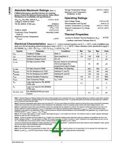
Absolute Maximum Ratings (Note 1)
If Military/Aerospace specified devices are required,
please contact the National Semiconductor Sales Office/
Distributors for availability and specifications.
Operating Ratings
Input Voltage Range
Recommended Load Current
Junction Temperature (TJ) Range
Ambient Temperature (TA) Range
ꢀ(Note 3)
PVIN, VDD Pin, SW1, SW2 & VOUT
:
−0.2V to +6.0V
2.5V to 5.5V
0mA to 1A
−40°C to +125°C
−40°C to +85°C
Voltage to SGND & PGND
FB, EN ,MODE, SYNC pins:
(PGND &
SGND-0.2V) to
(PVIN + 0.2)
PGND to SGND
-0.2V to 0.2V
Continuous Power Dissipation
ꢀ(Note 3)
Internally Limited
Thermal Properties
Junction-to-Ambient Thermal Resistance (θJA),
Maximum Junction Temperature
34°C/W
(TJ-MAX
)
+125°C
Leadless Lead frame Package (Note 5)
Electrical Characteristics (Notes 6, 7) Limits in standard typeface are for TJ = +25°C. Limits in boldface type
apply over the full operating ambient temperature range (−40°C ≤ = TA ≤ +85°C). Unless otherwise noted, specifications apply to
the LM3668. VIN = 3.6V = EN, VOUT = 3.3V. For VOUT = 4.5/5.0V, VIN = 4V.
Symbol
Parameter
Feedback Voltage
Conditions
Min
-3
Typ
Max
3
Units
%
VFB
ILIM
(Note 7)
Switch Peak Current Limit
Shutdown Supply Current
DC Bias Current in PFM
Open loop(Note 2)
EN =0V
1.6
1.85
0.01
2.05
1
A
ISHDN
µA
IQ_PFM
No load, device is not switching
(FB forced higher than
45
60
µA
programmed output voltage)
IQ_PWM
RDSON(P)
RDSON(N)
FOSC
DC Bias Current in PWM
Pin-Pin Resistance for PFET
Pin-Pin Resistance for NFET
Internal Oscillator Frequency
Sync Frequency Range
PWM Mode, No Switching
Switches P1 and P2
Switches N1 and N2
PWM Mode
600
130
100
2.2
750
180
150
2.5
µA
mΩ
mΩ
1.9
MHz
MHz
FSYNC
VIH
VIN = 3.6V
1.6
2.7
Logic High Input for EN, MODE/
SYNC pins
1.1
V
V
VIL
Logic Low Input for EN, MODES/
SYNC pins
0.4
1
IEN, MODE, SYNC
EN, MODES/SYNC pins Input
Current
0.3
µA
Note 1: Absolute Maximum Ratings indicate limits beyond which damage to the component may occur. Operating Ratings are conditions under which operation
of the device is guaranteed. Operating Ratings do not imply guaranteed performance limits. For guaranteed performance limits and associated test conditions,
see the Electrical Characteristics tables.
Note 2: Electrical Characteristic table reflects open loop data (FB = 0V and current drawn from SW pin ramped up until cycle by cycle current limits is activated).
Closed loop current limit is the peak inductor current measured in the application circuit by increasing output current until output voltage drops by 10%.
Note 3: In applications where high power dissipation and/or poor package thermal resistance is present, the maximum ambient temperature may have to be
derated. Maximum ambient temperature (TA-MAX) is dependent on the maximum operating junction temperature (TJ-MAX-OP = 125ºC), the maximum power
dissipation of the device in the application (PD-MAX), and the junction-to ambient thermal resistance of the part/package in the application (θJA), as given by the
following equation: TA-MAX = TJ-MAX-OP – (θJA × PD-MAX).
Note 4: The Human body model is a 100pF capacitor discharged through a 1.5 kΩ resistor into each pin. The machine model is a 200pF capacitor discharged
directly into each pin. MIL-STD-883 3015.7
Note 5: Junction-to-ambient thermal resistance (θJA) is taken from a thermal modeling result, performed under the conditions and guidelines set forth in the
JEDEC standard JESD51-7. The test board is a 4-layer FR-4 board measuring 101.6mm x 76.2mm x 1.6mm. Thickness of the copper layers are 2oz/1oz/1oz/
2oz. The middle layer of the board is 60mm x 60mm. Ambient temperature in simulation is 22°C, still air.
Junction-to-ambient thermal resistance is highly application and board-layout dependent. In applications where high maximum power dissipation exists, special
care must be paid to thermal dissipation issues in board design.
Note 6: All voltage is with respect to SGND.
Note 7: Min and Max limits are guaranteed by design, test, or statistical analysis. Typical numbers are not guaranteed, but do represent the most likely norm.
Note 8: CIN and COUT: Low-ESR Surface-Mount Ceramic Capacitors (MLCCs) used in setting electrical characteristics.
www.national.com
4

 NSC [ National Semiconductor ]