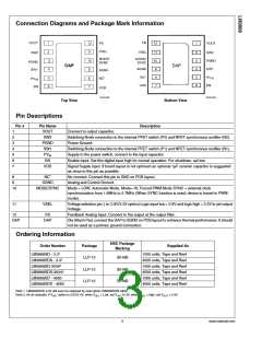
Connection Diagrams and Package Mark Information
20191402
20191403
Top View
Bottom View
Pin Descriptions
Pin #
Pin Name
VOUT
SW2
Description
1
2
3
4
5
6
7
Connect to output capacitor.
Switching Node connection to the internal PFET switch (P2) and NFET synchronous rectifier (N2).
Power Ground.
PGND
SW1
Switching Node connection to the internal PFET switch (P1) and NFET synchronous rectifier (N1).
Supply to the power switch, connect to the input capacitor.
PVIN
EN
Enable Input. Set this digital input high for normal operation. For shutdown, set low.
VDD
Signal Supply input. If board layout is not optimum an optional 1µF ceramic capacitor is suggested
as close to this pin as possible.
8
9
NC*
SGND
No connect. Connect this pin to GND on PCB layout.
Analog and Control Ground.
10
MODE/SYNC
Mode = LOW, Automatic Mode. Mode= HI, Forced PWM Mode SYNC = external clock
synchronization from 1.6MHz to 2.7MHz (When SYNC function is used, device is forced in PWM
mode).
11
VSEL
Voltage selection pin; ( ie: 2.8V/3.3V option) Logic input low = 2.8V and logic high = 3.3V to set output
Voltage.
12
FB
Feedback Analog Input. Connect to the output at the output filter.
DAP
DAP
Die Attach Pad, connect the DAP to SGND on PCB layout to enhance thermal performance. It should
not be used as a primary ground connection.
Ordering Information
NSC Package
Marking
Order Number
Package
Supplied As
LM3668SD - 3.31
LM3668SDX - 3.31
LM3668SD-30342
LM3668SDX-30342
LM3668SD - 4550
LM3668SDX - 4550
1000 units, Tape and Reel
4500 units, Tape and Reel
1000 units, Tape and Reel
4500 units, Tape and Reel
1000 units, Tape and Reel
4500 units, Tape and Reel
LLP-12
S016B
S018B
S019B
LLP-12
LLP-12
Note 1: LM3668SD/X-3.3V will soon be replaced by new option LM3668SD/X-2833.
Note 2: As an example, if VOUT option is 3.0V/3.4V, when VSEL = Low, set VOUT to 3V; when VSEL = high, set VOUT = 3.4V.
3
www.national.com

 NSC [ National Semiconductor ]