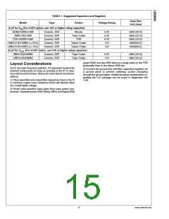
Circuit Description
The LM3668, a high-efficiency Buck or Boost DC-DC con-
verter, delivers a constant voltage from either a single Li-Ion
or three cell NIMH/NiCd battery to portable devices such as
mobile phones and PDAs. Using a voltage mode architecture
with synchronous rectification, the LM3668 has the ability to
deliver up to 1A depending on the input voltage, output volt-
age, ambient temperature and the chosen inductor.
20191406
In addition, the device incorporates a seamless transition
from buck-to-boost or boost-to-buck mode. The internal error
amplifier continuously monitors the output to determine the
transition from buck-to-boost or boost-to-buck operation. Fig-
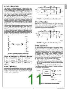
ure 2 shows the four switches network used for the buck and
boost operation. Table 1 summarizes the state of the switches
in different modes.
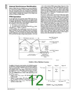
FIGURE 3. Simplified Circuit for Buck Operation
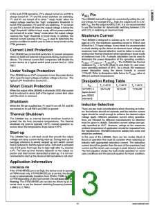
Boost Operation
When the input voltage is smaller than the output voltage, the
device enters boost mode operation where P1 is always ON,
while switches N2 & P2 control the output. Figure 4 shows the
simplified circuit for boost mode operation.
There are three modes of operation depending on the current
required: PWM (Pulse Width Modulation), PFM (Pulse Fre-
quency Modulation), and shutdown. The device operates in
PWM mode at load currents of approximately 80mA or higher
to improve efficiency. Lighter load current causes the device
to automatically switch into PFM mode to reduce current con-
sumption and extend battery life. Shutdown mode turns off
the device, offering the lowest current consumption.
20191408
FIGURE 4. Simplified Circuit for Boost Operation
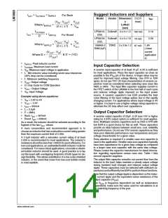
PWM Operation
In PWM operation, the output voltage is regulated by switch-
ing at a constant frequency and then modulating the energy
per cycle to control power to the load. In Normal operation,
the internal error amplifier provides an error signal, Vc, from
the feedback voltage and Vref. The error amplifier signal, Vc,
is compared with a voltage, Vcenter, and used to generate
the PWM signals for both Buck & Boost modes. Signal Vcen-
ter is a DC signal which sets the transition point of the buck
and boost modes. Below are three regions of operation:
20191405
FIGURE 2. Simplified Diagram of Switches
State of Switches in Different Modes
Mode
Always ON
Always
OFF
Switching
•
•
Region I: If Vc is less than Vcenter, Buck mode.
Region II: If Vc and Vcenter are equal, both PMOS
switches (P1, P2) are on and both NMOS switches (N1,
N2) are off. The power passes directly from input to output
via P1 & P2
Buck
SW P2
SW P1
SW N2
SW N1
SW P1 & N1
SW N2 & P2
Boost
TABLE 1
•
Region III: If Vc is greater than Vcenter, Boost mode.
The Buck-Boost operation is avoided, to improve the efficien-
cy across VIN and load range.
Buck Operation
When the input voltage is greater than the output voltage, the
device operates in buck mode where switch P2 is always ON
and P1 & N1 control the output . Figure 3 shows the simplified
circuit for buck mode operation.
20191415
FIGURE 5. PWM Generator Block Diagram
11
www.national.com

 NSC [ National Semiconductor ]