•
Avoid vias as much as possible. If vias are used, use mul-
tiple vias in parallel and/or make them as large as pos-
sible.
Application Information (Continued)
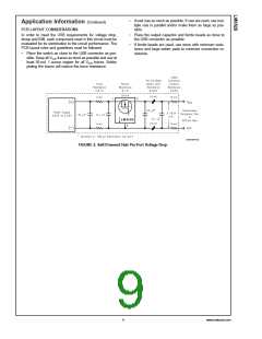
PCB LAYOUT CONSIDERATIONS
In order to meet the USB requirements for voltage drop,
droop and EMI, each component used in this circuit must be
evaluated for its contribution to the circuit performance. The
PCB layout rules and guidelines must be followed.
•
•
Place the output capacitor and ferrite beads as close to
the USB connector as possible.
If ferrite beads are used, use wires with minimum resis-
tance and large solder pads to minimize connection re-
sistance.
•
Place the switch as close to the USB connector as pos-
sible. Keep all Vbus traces as short as possible and use at
least 50-mil, 1 ounce copper for all Vbus traces. Solder
plating the traces will reduce the trace resistance.
DS101097-23
FIGURE 2. Self-Powered Hub Per-Port Voltage Drop
9
www.national.com

 NSC [ National Semiconductor ]