Absolute Maximum Ratings (Note 1)
Operating Ratings
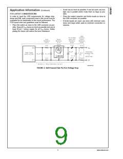
If Military/Aerospace specified devices are required,
please contact the National Semiconductor Sales Office/
Distributors for availability and specifications.
Supply Voltage Range
2.7V to 5.5V
Operating Ambient Range
−40˚C to 85˚C
Operating Junction Temperature
Range
Supply Voltage
−0.3V to 6V
−0.3V to 6V
−40˚C to 125˚C
−65˚C to +150˚C
Output Voltage
Storage Temperature Range
Voltage at All Other Pins
−0.3V to 5.5V
Lead Temperature
Power Dissipation (TA = 25˚C)
(Note 2)
(Soldering, 5 seconds)
260˚C
700 mW
160˚C
ESD Rating (Note 3)
ESD Rating Output Only
2kV
8kV
TJMAX (Note 2)
DC Electrical Characteristics
=
Limits in standard typeface are for TJ 25˚C, and limits in boldface type apply over the full operating temperature range. Un-
=
=
=
less otherwise specified: VIN 5.0V, VEN 0V (LM3526-L) or VEN VIN (LM3526-H).
Symbol Parameter Conditions
Min
Typ
100
110
Max
140
180
Units
mΩ
A
=
=
VIN 5V, IOUT 500mA, each switch
RON
IOUT
ISC
On Resistance
=
=
VIN 2.7V, IOUT 500mA, each switch
OUT pins continuous
output current
Each Output
0.5
Short Circuit Output
Current
Each Output (enable into Load) (Note 4)
VOUT 4.0V
A
=
0.5
1.2
1
1.9
1.5
=
VOUT 0.1V
OCTHRESH Over-current Threshold
2.2
3.2
10
A
ILEAK
OUT pins Output
Leakage Current
VEN = VIN (LM3526-L)
VEN = 0V (LM3526-H)
0.01
µA
=
IFO = 10 mA, VIN 5.0V
10
11
12
25
35
40
0.5
=
RFO
FLAG Output Voltage
IFO = 10 mA, VIN 3.3V
Ω
=
IFO = 10 mA, VIN 2.7V
IEN
EN/EN Leakage Current
EN/EN Input Logic High
EN/EN Input Logic Low
VEN/VEN = 0V or VEN/VEN = VIN
−0.5
µA
V
VIH
(Note 5)
(Note 5)
2.4
1.9
1.7
1.8
VIL
0.8
V
VUVLO
Under-Voltage Lockout
Threshold
V
IDDOFF
Supply Current
Switch-Off
0.2
1
µA
−40˚C ≤ TJ ≤ 85˚C
2
IDDON
ThSD
Supply Current
Switch-On
115
200
µA
˚C
Over-temperature
Shutdown Threshold
TJ Increasing, with no shorted output
TJ Increasing, with shorted output (s)
TJ Decreasing (Note 4)
150
145
135
=
IFH
Error Flag Leakage
Current
Vflag 5V
0.01
1
µA
Note 1: Absolute Maximum Ratings indicate limits beyond which damage to the device may occur. Electrical specifications do not apply when operating the device
beyond its rated operating conditions.
Note 2: The maximum power dissipation must be derated at elevated temperatures and is dictated by T
(Maximum junction temperature), θ (junction to am-
JA
JMAX
=
bient thermal resistance), and T (ambient temperature). The maximum allowable power dissipation at any temperature is P
(T
− T )/θ or the number
A
DMAX
JMAX A JA
=
given in the Absolute Maximum Ratings, which ever is lower. θ
150˚C/W.
JA
Note 3: The human body model is a 100 pF capacitor discharged through a 1.5 kΩ resistor into each pin. Enable pin ESD threshold is 1.7kV.
Note 4: Thermal Shutdown will protect the device from permanent damage.
Note 5: For LM3526-L, OFF is EN ≥ 2.4V and ON is EN ≤ 0.8V. For LM3526-H, OFF is EN ≤ 0.8V and ON is EN ≥ 2.4V.
3
www.national.com

 NSC [ National Semiconductor ]