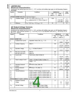
All Output Voltage Versions
Electrical Characteristics (Continued)
Specifications with standard type face are for TJ = 25˚C, and those with boldface type apply over full Operating Tempera-
ture Range. Unless otherwise specified, VIN = 12V for the 3.3V, 5V, and Adjustable version and VIN = 24V for the 12V ver-
sion. ILOAD = 200 mA
Symbol
Parameter
Conditions
LM2598-XX
Units
(Limits)
Typ
Limit
(Note 4)
(Note 5)
SHUTDOWN/SOFT-START CONTROL Test Circuit of Figure 1
ISD
Shutdown Current
VSHUTDOWN = 0.5V
5
µA
10
5
µA(max)
µA
ISS
Soft-start Current
VSoft-start = 2.5V
1.6
µA(max)
FLAG/DELAY CONTROL Test Circuit of Figure 1
Regulator Dropout Detector Low (Flag ON)
Threshold Voltage
96
%
%(min)
%(max)
V
92
98
VFSAT
IFL
Flag Output Saturation
Voltage
ISINK = 3 mA
VDELAY = 0.5V
VFLAG = 40V
0.3
0.7/1.0
V(max)
µA
Flag Output Leakage
Current
0.3
Delay Pin Threshold
Voltage
1.25
V
Low (Flag ON)
1.21
1.29
V(min)
V(max)
µA
High (Flag OFF) and VOUT Regulated
VDELAY = 0.5V
Delay Pin Source Current
Delay Pin Saturation
3
6
µA(max)
mV
Low (Flag ON)
55
350/400
mV(max)
Note 1: Absolute Maximum Ratings indicate limits beyond which damage to the device may occur. Operating Ratings indicate conditions for which the device is
intended to be functional, but do not guarantee specific performance limits. For guaranteed specifications and test conditions, see the Electrical Characteristics.
Note 2: Voltage internally clamped. If clamp voltage is exceeded, limit current to a maximum of 1 mA.
Note 3: The human body model is a 100 pF capacitor discharged through a 1.5k resistor into each pin.
Note 4: Typical numbers are at 25˚C and represent the most likely norm.
Note 5: All limits guaranteed at room temperature (standard type face) and at temperature extremes (bold type face). All room temperature limits are 100%
production tested. All limits at temperature extremes are guaranteed via correlation using standard Statistical Quality Control (SQC) methods. All limits are used
to calculate Average Outgoing Quality Level (AOQL).
Note 6: External components such as the catch diode, inductor, input and output capacitors can affect switching regulator system performance. When the LM2598
is used as shown in the Figure 1 test circuit, system performance will be as shown in system parameters section of Electrical Characteristics.
Note 7: The switching frequency is reduced when the second stage current limit is activated. The amount of reduction is determined by the severity of current
overload.
Note 8: No diode, inductor or capacitor connected to output pin.
Note 9: Feedback pin removed from output and connected to 0V to force the output transistor switch ON.
Note 10: Feedback pin removed from output and connected to 12V for the 3.3V, 5V, and the ADJ. version, and 15V for the 12V version, to force the output transistor
switch OFF.
Note 11: V = 40V.
IN
Note 12: Junction to ambient thermal resistance (no external heat sink) for the TO-220 package mounted vertically, with the leads soldered to a printed circuit board
2
with (1 oz.) copper area of approximately 1 in .
2
Note 13: Junction to ambient thermal resistance with the TO-263 package tab soldered to a single sided printed circuit board with 0.5 in of (1 oz.) copper area.
2
Note 14: Junction to ambient thermal resistance with the TO-263 package tab soldered to a single sided printed circuit board with 2.5 in of (1 oz.) copper area.
2
Note 15: Junction to ambient thermal resistance with the TO-263 package tab soldered to a double sided printed circuit board with 3 in of (1 oz.) copper area on
2
the LM2598S side of the board, and approximately 16 in of copper on the other side of the p-c board. See application hints in this data sheet and the thermal model
in Switchers Made Simple® version 4.2 software.
5
www.national.com

 NSC [ National Semiconductor ]