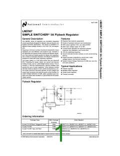
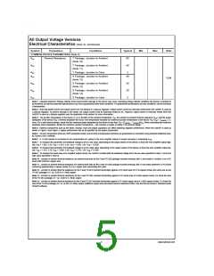
Absolute Maximum Ratings (Note 1)
If Military/Aerospace specified devices are required,
please contact the National Semiconductor Sales Office/
Distributors for availability and specifications.
Maximum Junction
Temperature (Note 3)
Power Dissipation (Note 3)
Minimum ESD Rating
150˚C
Internally Limited
=
=
(C 100 pF, R 1.5 kΩ
2 kV
Input Voltage
−0.4V ≤ VIN ≤ 45V
−0.4V ≤ VSW ≤ 65V
Internally Limited
Switch Voltage
Operating Ratings
Supply Voltage
Switch Current (Note 2)
Compensation Pin Voltage
Feedback Pin Voltage
Storage Temperature Range
Lead Temperature
−0.4V ≤ VCOMP ≤ 2.4V
−0.4V ≤ VFB ≤ 2 VOUT
−65˚C to +150˚C
4V ≤ VIN ≤ 40V
0V ≤ VSW ≤ 60V
ISW ≤ 5.0A
Output Switch Voltage
Output Switch Current
Junction Temperature Range
−40˚C ≤ TJ ≤ +125˚C
(Soldering, 10 sec.)
260˚C
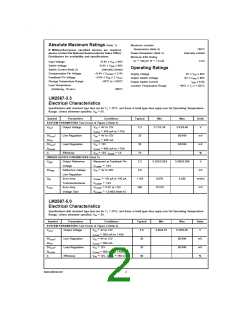
LM2587-3.3
Electrical Characteristics
=
Specifications with standard type face are for TJ 25˚C, and those in bold type face apply over full Operating Temperature
=
Range. Unless otherwise specified, VIN 5V.
Symbol
Parameters
Conditions
Typical
3.3
Min
Max
3.43/3.46
50/100
50/100
Units
V
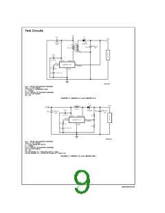
SYSTEM PARAMETERS Test Circuit of Figure 2 (Note 4)
=
VOUT
Output Voltage
Line Regulation
Load Regulation
Efficiency
VIN 4V to 12V
3.17/3.14
=
ILOAD 400 mA to 1.75A
=
∆VOUT
∆VIN
/
/
VIN 4V to 12V
20
mV
mV
%
=
ILOAD 400 mA
=
∆VOUT
VIN 12V
20
=
ILOAD 400 mA to 1.75A
∆ILOAD
=
=
η
VIN 12V, ILOAD 1A
75
UNIQUE DEVICE PARAMETERS (Note 5)
VREF
∆VREF
GM
Output Reference
Voltage
Measured at Feedback Pin
3.3
3.242/3.234
3.358/3.366
V
=
VCOMP 1.0V
=
Reference Voltage
Line Regulation
Error Amp
VIN 4V to 40V
2.0
mV
mmho
V/V
=
ICOMP −30 µA to +30 µA
1.193
260
0.678
2.259
=
VCOMP 1.0V
Transconductance
Error Amp
=
AVOL
VCOMP 0.5V to 1.6V
151/75
=
RCOMP 1.0 MΩ (Note 6)
Voltage Gain
LM2587-5.0
Electrical Characteristics
=
Specifications with standard type face are for TJ 25˚C, and those in bold type face apply over full Operating Temperature
=
Range. Unless otherwise specified, VIN 5V.
Symbol
Parameters
Conditions
Typical
5.0
Min
Max
5.20/5.25
50/100
50/100
Units
V
SYSTEM PARAMETERS Test Circuit of Figure 2 (Note 4)
=
VOUT
Output Voltage
Line Regulation
Load Regulation
Efficiency
VIN 4V to 12V
4.80/4.75
=
ILOAD 500 mA to 1.45A
=
∆VOUT
/
/
VIN 4V to 12V
20
mV
mV
%
=
∆VIN
ILOAD 500 mA
=
∆VOUT
VIN 12V
20
=
ILOAD 500 mA to 1.45A
∆ILOAD
=
=
η
VIN 12V, ILOAD 750 mA
80
www.national.com
2

 NSC [ National Semiconductor ]