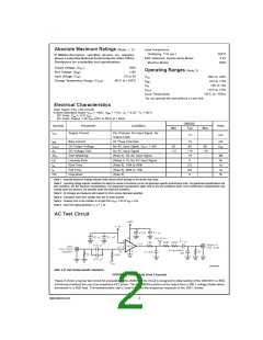
Application Hints (Continued)
DS101044-10
FIGURE 9. One Channel of the LM2435 with the Recommended Application Circuit
OPTIMIZING TRANSIENT RESPONSE
cation. The designer should note that if the load capacitance
is increased the AC component of the total power dissipation
will also increase.
Referring to Figure 9, there are three components (R1, R2
and L1) that can be adjusted to optimize the transient re-
sponse of the application circuit. Increasing the values of R1
and R2 will slow the circuit down while decreasing over-
shoot. Increasing the value of L1 will speed up the circuit as
well as increase overshoot. It is very important to use induc-
tors with very high self-resonant frequencies, preferably
above 300 MHz. Ferrite core inductors from J.W. Miller Mag-
netics (part # 78FR22K) were used for optimizing the perfor-
mance of the device in the NSC application board. The val-
ues shown in Figure 9 can be used as a good starting point
for the evaluation of the LM2435. Using a variable resistor
for R1 will simplify finding the value needed for optimum per-
formance in a given application. Once the optimum values
are determined the variable resistor can be replaced with
fixed values.
The LM2435 case temperature must be maintained below
100˚C. If the maximum expected ambient temperature is
70˚C and the maximum power dissipation is 8.7W (from Fig-
ure 6, 72.5 MHz bandwidth) then a maximum heat sink ther-
mal resistance can be calculated:
This example assumes a capacitive load of 8 pF and no re-
sistive load.
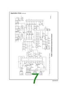
TYPICAL APPLICATION
A typical application of the LM2435 is shown in Figure 10.
Used in conjunction with an LM1279, a complete video chan-
nel from monitor input to CRT cathode can be achieved. Per-
formance is ideal for 1280 x 1024 resolution displays with
pixel clock frequencies up to 135 MHz. Figure 10 is the sche-
matic for the NSC demonstration board that can be used to
evaluate the LM1279/2435 combination in a monitor.
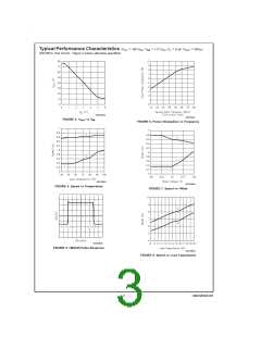
EFFECT OF LOAD CAPACITANCE
Figure 8 shows the effect of increased load capacitance on
the speed of the device. This demonstrates the importance
of knowing the load capacitance in the application.
EFFECT OF OFFSET
PC BOARD LAYOUT CONSIDERATIONS
Figure 7 shows the variation in rise and fall times when the
For optimum performance, an adequate ground plane, isola-
tion between channels, good supply bypassing and minimiz-
ing unwanted feedback are necessary. Also, the length of the
signal traces from the preamplifier to the LM2435 and from
the LM2435 to the CRT cathode should be as short as pos-
sible. The following references are recommended:
output offset of the device is varied from 40 VDC to 50 VDC
.
The rise time shows a maximum variation relative to the cen-
ter data point (45 VDC) of about 13%. The fall time shows a
maximum variation of about 3% relative to the center data
point.
Ott, Henry W., “Noise Reduction Techniques in Electronic
Systems”, John Wiley & Sons, New York, 1976.
THERMAL CONSIDERATIONS
Figure 4 shows the performance of the LM2435 in the test
circuit shown in Figure 2 as a function of case temperature.
The figure shows that the rise time of the LM2435 increases
by approximately 12% as the case temperature increases
from 50˚C to 100˚C. This corresponds to a speed degrada-
tion of 2.4% for every 10˚C rise in case temperature. There
is a negligible change in fall time vs. temperature in the test
circuit.
“Video Amplifier Design for Computer Monitors”, National
Semiconductor Application Note 1013.
Pease, Robert A., “Troubleshooting Analog Circuits”,
Butterworth-Heinemann, 1991.
Because of its high small signal bandwidth, the part may os-
cillate in a monitor if feedback occurs around the video chan-
nel through the chassis wiring. To prevent this, leads to the
video amplifier input circuit should be shielded, and input cir-
cuit wiring should be spaced as far as possible from output
circuit wiring.
Figure
6 shows the maximum power dissipation of the
LM2435 vs Frequency when all three channels of the device
are driving an 8 pF load with a 40 Vp-p alternating one pixel
on, one pixel off signal. The graph assumes a 72% active
time (device operating at the specified frequency) which is
typical in a monitor application. The other 28% of the time
the device is assumed to be sitting at the black level (65V in
this case). This graph gives the designer the information
needed to determine the heat sink requirement for the appli-
It is very important that the tab of the heatsink is connected
to PCB ground. The single ground pin does not provide an
adequate return path at high frequencies. The ground con-
nection can be made using the heatsink. The NSC LM1279
& LM243X (Nov. 1998, Rev. B) demo board, shown in Figure
11 and Figure 12, provides a good example of how this can
be done. A Thermalloy 6698B heatsink is used in the demo
5
www.national.com

 NSC [ National Semiconductor ]