Absolute Maximum Ratings (Notes 1, 3)
If Military/Aerospace specified devices are required,
please contact the National Semiconductor Sales Office/
Distributors for availability and specifications.
Lead Temperature
<
(Soldering, 10 sec.)
300˚C
2 kV
ESD Tolerance, Human Body Model
Machine Model
250V
Supply Voltage, (VCC
Bias Voltage, (VBB
Input Voltage, (VIN
Storage Temperature Range, (TSTG
)
+90V
+16V
Operating Ranges (Note 2)
)
)
0V to 6V
VCC
+60V to +85V
+8V to +15V
)
−65˚C to +150˚C
VBB
VIN
+0V to +5V
VOUT
+15V to +75V
−20˚C to +100˚C
Case Temperature
Do not operate the part without a heat sink.
Electrical Characteristics
(See Figure 2 for Test Circuit)
Unless otherwise noted: VCC = +80V, VBB = +12V, CL = 8 pF, TC = 50˚C
DC Tests: VIN = +2.8 VDC
AC Tests: Output = 40 VPP (25V to 65V) at 1 MHz.
LM2435
Typ
Symbol
Parameter
Supply Current
Condition
Units
Max
Min
ICC
Per Channel, No Input Signal, No
Output Load
13
mA
IBB
VOUT
AV
Bias Current
DC Output Voltage
DC Voltage Gain
Gain Matching
Linearity Error
Rise Time
All Three Channels
14
65
−14
1.0
8
mA
No AC Input Signal, VIN = 1.35V
No AC Input Signal
62
68
VDC
−12
−16
∆AV
LE
(Note 4), No AC Input Signal
(Notes 4, 5), No AC Input Signal
(Note 6), 10% to 90%
(Note 6), 90% to 10%
(Note 6)
dB
%
tR
5.5
6.0
5
ns
ns
%
tF
Fall Time
OS
Overshoot
Note 1: Absolute Maximum Ratings indicate limits beyond which damage to the device may occur.
Note 2: Operating ratings indicate conditions for which the device is functional, but do not guarantee specific performance limits. For guaranteed specifications and
test conditions, see the Electrical Characteristics. The guaranteed specifications apply only for the test conditions listed. Some performance characteristics may
change when the device is not operated under the listed test conditions.
Note 3: All voltages are measured with respect to GND, unless otherwise specified.
Note 4: Calculated value from Voltage Gain test on each channel.
Note 5: Linearity Error is the variation in dc gain from V = 1.0V to V = 4.5V.
IN IN
<
f
Note 6: Input from signal generator: t , t
1 ns.
r
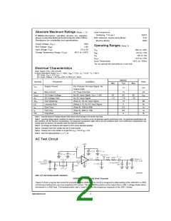
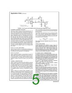
AC Test Circuit
DS101044-3
Note: 8 pF load includes parasitic capacitance.
FIGURE 2. Test Circuit (One Channel)
Figure 2 shows a typical test circuit for evaluation of the LM2435. This circuit is designed to allow testing of the LM2435 in a 50Ω
environment without the use of an expensive FET probe. The two 2490Ω resistors at the output form a 200:1 voltage divider when
connected to a 50Ω load. The compensation cap is used to flatten the frequency response of the 200:1 divider.
www.national.com
2

 NSC [ National Semiconductor ]