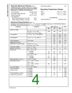
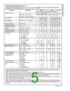
Absolute Maximum Ratings (Note 1)
If Military/Aerospace specified devices are required,
please contact the National Semiconductor Sales Office/
Distributors for availability and specifications.
ESD Tolerance (Note 5)
3 kV
Operating Temperature Range
LM117
LM317A
LM317
−55˚C ≤ TJ ≤ +150˚C
−40˚C ≤ TJ ≤ +125˚C
0˚C ≤ TJ ≤ +125˚C
Power Dissipation
Internally Limited
+40V, −0.3V
Input-Output Voltage Differential
Storage Temperature
Lead Temperature
−65˚C to +150˚C
Preconditioning
Thermal Limit Burn-In
Metal Package (Soldering, 10 seconds)
Plastic Package (Soldering, 4 seconds)
300˚C
260˚C
All Devices 100%
Electrical Characteristics (Note 3)
Specifications with standard type face are for TJ = 25˚C, and those with boldface type apply over full Operating Tempera-
ture Range. Unless otherwise specified, VIN − VOUT = 5V, and IOUT = 10 mA.
Parameter
Conditions
LM117 (Note 2)
Units
Min
Typ
Max
1.30
Reference Voltage
V
V
3V ≤ (VIN − VOUT) ≤ 40V,
1.20
1.25
10 mA ≤ IOUT ≤ IMAX, P ≤ PMAX
3V ≤ (VIN − VOUT) ≤ 40V (Note 4)
Line Regulation
Load Regulation
0.01
0.02
0.1
0.02
0.05
0.3
1
%/V
%/V
%
10 mA ≤ IOUT ≤ IMAX (Note 4)
0.3
%
Thermal Regulation
20 ms Pulse
0.03
50
0.07
100
5
%/W
µA
Adjustment Pin Current
Adjustment Pin Current Change
10 mA ≤ IOUT ≤ IMAX
3V ≤ (VIN − VOUT) ≤ 40V
TMIN ≤ TJ ≤ TMAX
(VIN − VOUT) = 40V
(VIN − VOUT) ≤ 15V
K Package
0.2
µA
Temperature Stability
Minimum Load Current
Current Limit
1
%
3.5
5
mA
1.5
0.5
2.2
0.8
3.4
1.8
A
A
H Package
(VIN − VOUT) = 40V
K Package
0.3
0.4
0.2
A
A
H Package
0.15
RMS Output Noise, % of VOUT
Ripple Rejection Ratio
10 Hz ≤ f ≤ 10 kHz
VOUT = 10V, f = 120 Hz,
CADJ = 0 µF
0.003
65
%
dB
VOUT = 10V, f = 120 Hz,
CADJ = 10 µF
66
80
dB
Long-Term Stability
Thermal Resistance,
Junction-to-Case
TJ = 125˚C, 1000 hrs
K Package
0.3
2.3
12
1
3
%
˚C/W
˚C/W
˚C/W
˚C/W
˚C/W
˚C/W
H Package
15
E Package
Thermal Resistance, Junction-
to-Ambient (No Heat Sink)
K Package
35
H Package
140
E Package
www.national.com
4

 NSC [ National Semiconductor ]