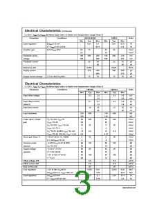
Electrical Characteristics (Continued)
=
TJ 25˚C, TMIN≤TJ≤TMAX (Boldface type refers to limits over temperature range) (Note 5)
Parameter
Conditions
0.2V≤VREF≤5.5V
LM10BL
Typ
LM10CL
Typ
Units
Min
30
Max
Min
20
Max
Amplifier gain
70
70
V/mV
V/mV
mV
20
15
Feedback sense voltage
Feedback current
195
194
200
20
205
206
50
190
189
200
22
210
211
75
mV
nA
65
90
nA
Reference drift
Supply current
0.002
260
0.003
280
%/˚C
µA
400
500
500
570
µA
Note 1: Absolute Maximum Ratings indicate limits beyond which damage to the device may occur. Operating Ratings indicate conditions for which the device is func-
tional, but do not guarantee specific performance limits.
Note 2: The Input voltage can exceed the supply voltages provided that the voltage from the input to any other terminal does not exceed the maximum differential
−
<
input voltage and excess dissipation is accounted for when V
IN
V .
Note 3: The maximum, operating-junction temperature is 150˚C for the LM10, 100˚C for the LM10B(L) and 85˚C for the LM10C(L). At elevated temperatures, devices
must be derated based on package thermal resistance.
Note 4: Internal thermal limiting prevents excessive heating that could result in sudden failure, but the IC can be subjected to accelerated stress with a shorted output
and worst-case conditions.
−
+
=
=
40V
<
Note 5: These specifications apply for V ≤V ≤V −0.85V (1.0V), 1.2V (1.3V)
CM
V
≤V
MAX
, V
REF
0.2V and 0≤I
REF
≤1.0 mA, unless otherwise specified: V
MAX
S
for the standard part and 6.5V for the low voltage part. Normal typeface indicates 25˚C limits. Boldface type indicates limits and altered test conditions for
full-temperature-range operation; this is −55˚C to 125˚C for the LM10, −25˚C to 85˚C for the LM10B(L) and 0˚C to 70˚C for the LM10C(L). The specifications do
not include the effects of thermal gradients (τ 20 ms), die heating (τ 0.2s) or package heating. Gradient effects are small and tend to offset the electrical error (see
1
2
curves).
−
−
−
=
=
J
>
Note 6: For T 90˚C, I
may exceed 1.5 nA for V
V . With T 125˚C and V ≤V ≤V +0.1V, I ≤5 nA.
J
OS
CM
CM OS
+
Note 7: This defines operation in floating applications such as the bootstrapped regulator or two-wire transmitter. Output is connected to the V terminal of the IC
−
and input common mode is referred to V (see typical applications). Effect of larger output-voltage swings with higher load resistance can be accounted for by adding
the positive-supply rejection error.
Note 8: Refer to RETS10X for LM10H military specifications.
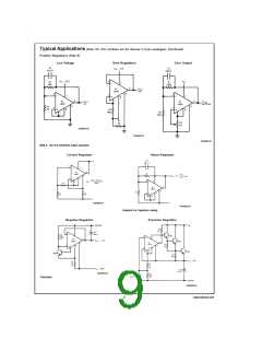
Definition of Terms
Input offset voltage: That voltage which must be applied
between the input terminals to bias the unloaded output in
the linear region.
Supply-voltage rejection: The ratio of the specified
supply-voltage change to the change in offset voltage be-
tween the extremes.
Input offset current: The difference in the currents at the in-
put terminals when the unloaded output is in the linear re-
gion.
Line regulation: The average change in reference output
voltage over the specified supply voltage range.
Load regulation: The change in reference output voltage
Input bias current: The absolute value of the average of the
two input currents.
from no load to that load specified.
Feedback sense voltage: The voltage, referred to V−, on
the reference feedback terminal while operating in regula-
tion.
Input resistance: The ratio of the change in input voltage to
the change in input current on either input with the other
grounded.
Reference amplifier gain: The ratio of the specified refer-
ence output change to the change in feedback sense voltage
required to produce it.
Large signal voltage gain: The ratio of the specified output
voltage swing to the change in differential input voltage re-
quired to produce it.
Feedback current: The absolute value of the current at the
Shunt gain: The ratio of the specified output voltage swing
to the change in differential input voltage required to produce
it with the output tied to the V+ terminal of the IC. The load
and power source are connected between the V+ and V− ter-
minals, and input common-mode is referred to the V− termi-
nal.
feedback terminal when operating in regulation.
Supply current: The current required from the power
source to operate the amplifier and reference with their out-
puts unloaded and operating in the linear range.
Common-mode rejection: The ratio of the input voltage
range to the change in offset voltage between the extremes.
www.national.com
4

 NSC [ National Semiconductor ]