Absolute Maximum Ratings (Note 11)
If Military/Aerospace specified devices are required,
please contact the National Semiconductor Sales Office/
Distributors for availability and specifications.
LF444A/LF444
(Note 4)
Operating Temperature Range
Storage Temperature Range
ESD Tolerance (Note 10)
−65˚C ≤ TA ≤ 150˚C
Rating to
be determined
LF444A
LF444
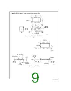
Soldering Information
Dual-In-Line Packages
(Soldering, 10 sec.)
Small Outline Package
Vapor Phase (60 sec.)
Infrared (15 sec.)
±
±
±
±
±
±
Supply Voltage
22V
38V
19V
18V
30V
15V
Differential Input Voltage
Input Voltage Range
(Note 1)
260˚C
215˚C
220˚C
Output Short Circuit
Duration (Note 2)
Continuous
Continuous
See AN-450 “Surface Mounting Methods and Their Effect on
Product Reliability” for other methods of soldering surface
mount devices.
D Package
N, M Packages
Power Dissipation
(Notes 3, 9)
Tj max
900 mW
670 mW
150˚C
115˚C
θjA (Typical)
100˚C/W
85˚C/W
DC Electrical Characteristics (Note 5)
Symbol
Parameter
Conditions
LF444A
Typ
LF444
Typ
3
Units
Min
Max
5
Min
Max
10
=
=
VOS
Input Offset Voltage
RS 10k, TA 25˚C
2
mV
mV
0˚C ≤ TA ≤ +70˚C
6.5
8
12
−55˚C ≤ TA ≤ +125˚C
mV
=
∆VOS/∆T
Average TC of Input
Offset Voltage
RS 10 kΩ
10
5
10
5
µV/˚C
=
=
±
IOS
Input Offset Current
VS
15V
Tj 25˚C
25
1.5
10
50
3
50
pA
nA
=
(Notes 5, 6)
Tj 70˚C
1.5
=
Tj 125˚C
nA
=
=
±
IB
Input Bias Current
VS
15V
Tj 25˚C
10
10
100
3
pA
=
(Notes 5, 6)
Tj 70˚C
nA
=
Tj 125˚C
20
nA
=
RIN
Input Resistance
Large Signal Voltage
Gain
Tj 25˚C
1012
100
1012
100
Ω
=
=
±
±
AVOL
VS
15V, VO
10V
50
25
25
15
V/mV
=
=
RL 10 kΩ, TA 25˚C
Over Temperature
V/mV
V
=
=
±
±
±
±
±
±
±
13
VO
Output Voltage Swing
Input Common-Mode
Voltage Range
VS
15V, RL 10 kΩ
12
16
13
12
11
VCM
+18
−17
100
+14
−12
95
V
V
CMRR
PSRR
IS
Common-Mode
Rejection Ratio
Supply Voltage
RS ≤ 10 kΩ
80
70
dB
(Note 7)
80
100
0.6
70
90
dB
Rejection Ratio
Supply Current
0.8
0.6
1.0
mA
www.national.com
2

 NSC [ National Semiconductor ]