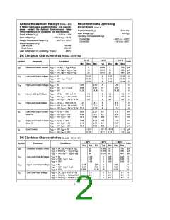
Truth Table
Division Ratio Table
State
Number of
Pin
Count
n
2
A
B
Counter Stages
n
0
1
5
6
9
Auto Reset Operating
Timer Operational
Auto Reset Disabled
Master Reset On
0
0
1
1
0
1
0
1
13
10
8
8192
1024
256
Output Initially Low
after Reset
Output Initially High
after Reset
16
65536
10
Single Cycle Mode
Recycle Mode
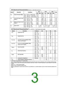
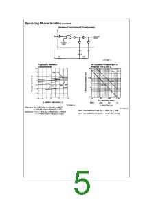
Operating Characteristics
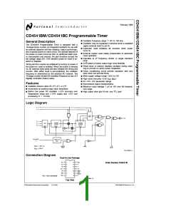
However, when B is ‘‘0’’, normal counting is interrupted and
the 9th counter stage receives its clock directly from the
8
oscillator (i.e., effectively outputting 2 ).
With Auto Reset pin set to a ‘‘0’’ the counter circuit is initial-
ized by turning on power. Or with power already on, the
counter circuit is reset when the Master Reset pin is set to a
‘‘1’’. Both types of reset will result in synchronously reset-
ting all counter stages independent of counter state.
The Q/Q select output control pin provides for a choice of
output level. When the counter is in a reset condition and
Q/Q select pin is set to a ‘‘0’’ the Q output is a ‘‘0’’. Corre-
spondingly, when Q/Q select pin is set to a ‘‘1’’ the Q output
is a ‘‘1’’.
The RC oscillator frequency is determined by the external
RC network, i.e.:
1
When the mode control pin is set to a ‘‘1’’, the selected
count is continually transmitted to the output. But, with
mode pin ‘‘0’’ and after a reset condition the RS flip-flop
resets (see Logic Diagram), counting commences and after
s
s
100 kHz)
e
f
if (1 kHz
f
2.3 R
C
tc tc
t
&
and R
2 R where R
tc
10 kX
S
S
b
n
1
The time select inputs (A and B) provide a two-bit address
10 13
2
to change state. Hence, after another 2
counts the RS flip-flop sets which causes the output
b
8
n
1
to output any one of four counter stages (2 , 2 , 2 , and
16
counts the out-
n
). The 2 counts as shown in the Division Ratio Table
represent the Q output of the Nth stage of the counter.
2
put will not change. Thus, a Master Reset pulse must be
applied or a change in the mode pin level is required to
reset the single cycle operation.
16
When A is ‘‘1’’, 2 is selected for both states of B.
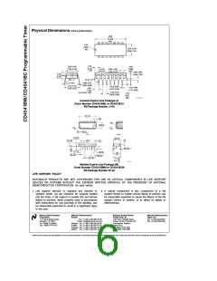
Power Dissipation Test
Circuit and Waveforms
Switching Time Test
Circuit and Waveforms
(R and C outputs are left open)
tc tc
TL/F/6001–4
TL/F/6001–3
TL/F/6001–5
TL/F/6001–6
4

 NSC [ National Semiconductor ]